What is Global Single Crystal AlN Substrate Wafer Market?
The Global Single Crystal AlN Substrate Wafer Market refers to the worldwide industry focused on the production and distribution of single crystal aluminum nitride (AlN) substrate wafers. These wafers are essential components in the manufacturing of various high-performance electronic devices. Single crystal AlN substrates are known for their excellent thermal conductivity, high electrical insulation, and superior mechanical properties, making them ideal for use in advanced technologies. The market encompasses a range of activities, including research and development, production, and sales of these wafers to various industries such as electronics, telecommunications, and power devices. The demand for single crystal AlN substrate wafers is driven by the growing need for efficient and reliable electronic components in various applications, including UVC LEDs, RF devices, and power devices. As technology continues to advance, the market for these high-quality substrates is expected to expand, offering new opportunities for innovation and growth.
Wafer Size: 20mm and Below, Wafer Size: 20mm-50mm, Wafer Size: 50 and Above in the Global Single Crystal AlN Substrate Wafer Market:
In the Global Single Crystal AlN Substrate Wafer Market, wafer sizes are categorized into three main segments: 20mm and below, 20mm-50mm, and 50mm and above. Each size category serves different applications and has unique characteristics. Wafers sized 20mm and below are typically used in specialized applications where precision and miniaturization are crucial. These smaller wafers are often employed in niche markets such as microelectronics and specific types of sensors. Their compact size allows for high precision in small-scale devices, making them ideal for applications that require detailed and intricate designs. On the other hand, wafers sized between 20mm and 50mm are more versatile and are used in a broader range of applications. This size range strikes a balance between performance and cost, making it suitable for mid-range electronic devices and components. These wafers are commonly used in the production of LEDs, RF devices, and other electronic components that require a moderate level of precision and performance. The largest category, wafers sized 50mm and above, is used in high-performance applications where maximum efficiency and reliability are paramount. These larger wafers are essential in the production of power devices and high-frequency RF devices, where their superior thermal and electrical properties can be fully utilized. The larger surface area of these wafers allows for the production of more substantial and more powerful electronic components, making them indispensable in industries that demand high performance and durability. Each wafer size category plays a critical role in the overall market, catering to different needs and applications, and driving innovation and growth in the field of advanced electronics.
UVC LED, RF Devices, Power Devices, Others in the Global Single Crystal AlN Substrate Wafer Market:
The usage of Global Single Crystal AlN Substrate Wafer Market spans several key areas, including UVC LEDs, RF devices, power devices, and others. In the realm of UVC LEDs, single crystal AlN substrate wafers are crucial due to their excellent thermal conductivity and high electrical insulation. These properties enable the efficient operation of UVC LEDs, which are used in sterilization and disinfection applications. The demand for UVC LEDs has surged, especially in the wake of global health concerns, driving the need for high-quality AlN substrates. In RF devices, which are used in telecommunications and wireless communication systems, single crystal AlN substrates provide the necessary thermal management and electrical insulation to ensure reliable performance. The high-frequency operation of RF devices generates significant heat, and the superior thermal properties of AlN substrates help dissipate this heat effectively, enhancing the device's longevity and performance. Power devices, which are used in power conversion and management systems, also benefit from the use of single crystal AlN substrates. These substrates can handle high power levels and provide excellent thermal management, making them ideal for use in power electronics. The efficiency and reliability of power devices are critical in applications such as electric vehicles, renewable energy systems, and industrial automation. Other applications of single crystal AlN substrate wafers include their use in sensors, laser diodes, and other advanced electronic components. The versatility and superior properties of AlN substrates make them suitable for a wide range of high-performance applications, driving their demand across various industries.
Global Single Crystal AlN Substrate Wafer Market Outlook:
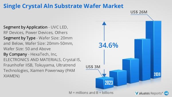
The global Single Crystal AlN Substrate Wafer market was valued at US$ 3 million in 2023 and is anticipated to reach US$ 26 million by 2030, witnessing a CAGR of 34.6% during the forecast period 2024-2030. This significant growth reflects the increasing demand for high-quality AlN substrates in various advanced electronic applications. The market's expansion is driven by the need for efficient thermal management and high electrical insulation in electronic devices, which are essential for their reliable performance and longevity. As industries such as telecommunications, power electronics, and healthcare continue to evolve and adopt more advanced technologies, the demand for single crystal AlN substrate wafers is expected to rise. The market outlook indicates a promising future for this industry, with substantial growth opportunities and potential for innovation.
| Report Metric | Details |
| Report Name | Single Crystal AlN Substrate Wafer Market |
| Accounted market size in 2023 | US$ 3 in million |
| Forecasted market size in 2030 | US$ 26 million |
| CAGR | 34.6% |
| Base Year | 2023 |
| Forecasted years | 2024 - 2030 |
| Segment by Type |
|
| Segment by Application |
|
| Production by Region |
|
| Consumption by Region |
|
| By Company | HexaTech, Inc, ELECTRONICS AND MATERIALS, Crystal IS, Fraunhofer IISB, Tokuyama, Ultratrend Technologies, Xiamen Powerway (PAM XIAMEN) |
| Forecast units | USD million in value |
| Report coverage | Revenue and volume forecast, company share, competitive landscape, growth factors and trends |


