What is Global Wafer Edge Ring Market?
The Global Wafer Edge Ring Market is a specialized segment within the semiconductor industry that focuses on the production and distribution of wafer edge rings. These rings are essential components used in various semiconductor manufacturing processes to protect the edges of silicon wafers from damage and contamination. Wafer edge rings are crucial in ensuring the integrity and quality of the wafers, which are the foundational elements in the production of integrated circuits and other semiconductor devices. The market for wafer edge rings is driven by the increasing demand for semiconductors in various applications, including consumer electronics, automotive, telecommunications, and industrial sectors. As technology advances and the need for more sophisticated and miniaturized electronic devices grows, the importance of wafer edge rings in maintaining the precision and reliability of semiconductor manufacturing processes becomes even more critical. The global market for wafer edge rings is characterized by a diverse range of materials and types, each designed to meet specific requirements and performance standards in different manufacturing environments.
Ceramic (SiC, AlN, etc.) Edge Ring, Quartz Wafer Edge Ring, Metal Wafer Edge Ring, PI (Polyimide) Edge Ring, CFRP Composites Edge Ring, Plastic (PEEK/PPS) Edge Ring in the Global Wafer Edge Ring Market:
Ceramic edge rings, such as those made from silicon carbide (SiC) and aluminum nitride (AlN), are highly valued in the Global Wafer Edge Ring Market for their exceptional thermal conductivity, mechanical strength, and resistance to chemical corrosion. These properties make ceramic edge rings ideal for high-temperature processes and environments where durability and stability are paramount. Quartz wafer edge rings, on the other hand, are known for their excellent thermal stability and low thermal expansion, making them suitable for processes that require precise temperature control and minimal thermal distortion. Metal wafer edge rings, typically made from materials like stainless steel or aluminum, offer robust mechanical strength and are often used in applications where physical durability is a primary concern. Polyimide (PI) edge rings are appreciated for their high thermal stability and chemical resistance, making them suitable for a variety of semiconductor manufacturing processes. CFRP (carbon fiber reinforced polymer) composites edge rings combine the lightweight properties of polymers with the strength of carbon fibers, providing a balance of durability and ease of handling. Plastic edge rings, such as those made from PEEK (polyether ether ketone) or PPS (polyphenylene sulfide), offer good chemical resistance and mechanical properties, making them versatile options for various applications. Each type of edge ring material brings unique advantages to the table, allowing manufacturers to choose the most appropriate solution based on the specific requirements of their processes and the operating conditions they face.
RTP Process, Etching Process, Mocvd Process, PVD Process, Others in the Global Wafer Edge Ring Market:
The Global Wafer Edge Ring Market finds extensive usage in several critical semiconductor manufacturing processes, including RTP (Rapid Thermal Processing), etching, MOCVD (Metal-Organic Chemical Vapor Deposition), PVD (Physical Vapor Deposition), and others. In the RTP process, wafer edge rings play a crucial role in ensuring uniform heating and cooling of the wafers, which is essential for achieving consistent and high-quality results. The edge rings help to minimize thermal gradients and prevent warping or cracking of the wafers during rapid temperature changes. In the etching process, wafer edge rings protect the wafer edges from being etched away, ensuring the integrity and precision of the patterns being created on the wafer surface. This is particularly important in the production of intricate and densely packed semiconductor devices. MOCVD processes, which are used to deposit thin films of materials onto the wafer surface, also benefit from the use of edge rings. These rings help to maintain a clean and controlled environment, preventing contamination and ensuring uniform film deposition. In PVD processes, wafer edge rings are used to protect the wafer edges from physical damage and contamination during the deposition of thin films. This helps to ensure the quality and reliability of the final semiconductor devices. Other processes, such as chemical mechanical planarization (CMP) and ion implantation, also rely on wafer edge rings to protect the wafer edges and maintain the precision and quality of the manufacturing process. Overall, the use of wafer edge rings in these various processes is essential for achieving the high levels of precision, reliability, and quality required in semiconductor manufacturing.
Global Wafer Edge Ring Market Outlook:
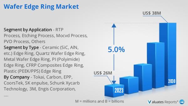
The global Wafer Edge Ring market was valued at US$ 26 million in 2023 and is anticipated to reach US$ 38 million by 2030, witnessing a CAGR of 5.0% during the forecast period from 2024 to 2030. According to SEMI, worldwide sales of semiconductor manufacturing equipment increased by 5% from $102.6 billion in 2021 to an all-time record of $107.6 billion in 2022. For the third consecutive year, China remained the largest semiconductor equipment market in 2022, despite a 5% slowdown in the pace of investments in the region year over year, accounting for $28.3 billion in billings.
| Report Metric | Details |
| Report Name | Wafer Edge Ring Market |
| Accounted market size in 2023 | US$ 26 million |
| Forecasted market size in 2030 | US$ 38 million |
| CAGR | 5.0% |
| Base Year | 2023 |
| Forecasted years | 2024 - 2030 |
| Segment by Type |
|
| Segment by Application |
|
| Production by Region |
|
| Consumption by Region |
|
| By Company | Tokai, Carbon, EPP, CoorsTek, SK enpulse, Schunk Xycarb Technology, 3M, Engis Corporation, Shen-Yueh Technology, Greene Tweed, CALITECH, Top Seiko Co., Ltd., Ensinger Grou, Sprint Precision Technologies Co., Ltd, KFMI, HCAT, KALLAX Company |
| Forecast units | USD million in value |
| Report coverage | Revenue and volume forecast, company share, competitive landscape, growth factors and trends |


