What is Global Semiconductor Process Chambers Market?
The global Semiconductor Process Chambers market is a specialized segment within the semiconductor manufacturing industry. These chambers are critical components used in the fabrication of semiconductor devices, which are essential for a wide range of electronic products. Semiconductor process chambers are designed to create controlled environments where various processes such as deposition, etching, and implantation can occur. These processes are fundamental to the creation of integrated circuits and other semiconductor devices. The market for these chambers is driven by the increasing demand for advanced electronic devices, including smartphones, computers, and automotive electronics. As technology continues to evolve, the need for more sophisticated and efficient semiconductor process chambers grows, making this market a vital part of the global electronics supply chain. The market is characterized by continuous innovation and development, with manufacturers striving to improve the performance and efficiency of their chambers to meet the ever-growing demands of the semiconductor industry.
Reaction Chamber, Transfer Chamber, Load Lock Chamber in the Global Semiconductor Process Chambers Market:
In the context of the Global Semiconductor Process Chambers Market, various types of chambers play distinct roles in the semiconductor manufacturing process. The Reaction Chamber is a critical component where chemical reactions occur to deposit thin films on semiconductor wafers. These chambers are designed to maintain precise temperature, pressure, and gas flow conditions to ensure uniform film deposition, which is essential for the performance and reliability of semiconductor devices. The Transfer Chamber, on the other hand, is used to move wafers between different process chambers without exposing them to the external environment. This is crucial for maintaining the integrity of the wafers and preventing contamination, which can adversely affect the quality of the final product. The Load Lock Chamber serves as an intermediary between the external environment and the vacuum environment of the process chambers. It allows wafers to be loaded and unloaded from the process chambers without compromising the vacuum conditions, which are essential for many semiconductor manufacturing processes. Each of these chambers plays a vital role in ensuring the efficiency and effectiveness of the semiconductor manufacturing process, contributing to the overall performance and yield of semiconductor devices. The integration and coordination of these chambers are critical for achieving the high levels of precision and control required in semiconductor fabrication. As the demand for more advanced and miniaturized semiconductor devices continues to grow, the importance of these chambers in the manufacturing process becomes even more pronounced. Manufacturers are continually innovating and improving the design and functionality of these chambers to meet the evolving needs of the semiconductor industry.
Thin Film (CVD, PVD and ALD), Etching, E-beam and Lithography, Implant, Others in the Global Semiconductor Process Chambers Market:
The Global Semiconductor Process Chambers Market finds extensive usage in various areas of semiconductor manufacturing, including Thin Film deposition, Etching, E-beam and Lithography, Implant, and others. In Thin Film deposition, processes such as Chemical Vapor Deposition (CVD), Physical Vapor Deposition (PVD), and Atomic Layer Deposition (ALD) are employed to create thin layers of materials on semiconductor wafers. These processes are essential for forming the various layers that make up semiconductor devices, and the precision and uniformity of the deposition are critical for device performance. Etching is another crucial process where material is selectively removed from the wafer to create the desired patterns and structures. This process requires highly controlled environments to ensure accuracy and prevent damage to the wafer. E-beam and Lithography are used to define the intricate patterns on the semiconductor wafers, which are essential for creating the circuits and components of semiconductor devices. These processes require extremely precise control and alignment to achieve the high levels of resolution needed for modern semiconductor devices. Implant processes involve the introduction of dopants into the semiconductor material to modify its electrical properties. This is a critical step in defining the functionality of semiconductor devices, and the process chambers used for implantation must provide precise control over the dose and energy of the implanted ions. Other processes in semiconductor manufacturing, such as cleaning and annealing, also rely on specialized process chambers to achieve the desired results. The versatility and precision of these chambers are essential for the successful fabrication of semiconductor devices, and their importance continues to grow as the industry advances towards more complex and miniaturized devices.
Global Semiconductor Process Chambers Market Outlook:
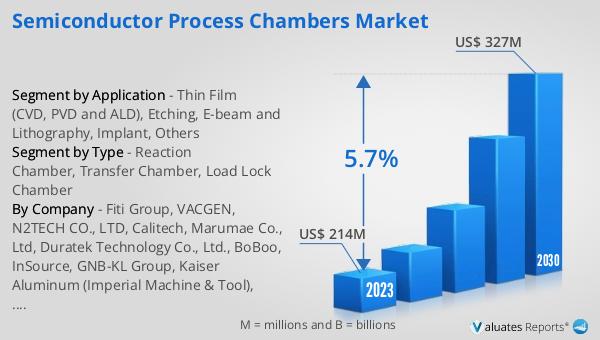
The global Semiconductor Process Chambers market was valued at US$ 214 million in 2023 and is anticipated to reach US$ 327 million by 2030, witnessing a CAGR of 5.7% during the forecast period 2024-2030. According to SEMI, worldwide sales of semiconductor manufacturing equipment increased 5% from $102.6 billion in 2021 to an all-time record of $107.6 billion in 2022. For the third consecutive year, China remained the largest semiconductor equipment market in 2022 despite a 5% slowdown in the pace of investments in the region year over year, accounting for $28.3 billion in billings. This growth reflects the ongoing demand for advanced semiconductor devices and the critical role that process chambers play in their fabrication. The continuous innovation and development in the design and functionality of these chambers are essential for meeting the evolving needs of the semiconductor industry. As the market continues to expand, manufacturers are focused on improving the performance and efficiency of their process chambers to support the production of next-generation semiconductor devices.
| Report Metric | Details |
| Report Name | Semiconductor Process Chambers Market |
| Accounted market size in 2023 | US$ 214 million |
| Forecasted market size in 2030 | US$ 327 million |
| CAGR | 5.7% |
| Base Year | 2023 |
| Forecasted years | 2024 - 2030 |
| Segment by Type |
|
| Segment by Application |
|
| Production by Region |
|
| Consumption by Region |
|
| By Company | Fiti Group, VACGEN, N2TECH CO., LTD, Calitech, Marumae Co., Ltd, Duratek Technology Co., Ltd., BoBoo, InSource, GNB-KL Group, Kaiser Aluminum (Imperial Machine & Tool), LACO Technologies, Sprint Precision Technologies Co., Ltd, KFMI, Shenyang Fortune Precision Equipment Co., Ltd, Tolerance Technology (Shanghai), Sanyue Semiconductor Technology |
| Forecast units | USD million in value |
| Report coverage | Revenue and volume forecast, company share, competitive landscape, growth factors and trends |


