What is Global Automated Optical Inspection (AOI) Equipment for IC Substrate Market?
Global Automated Optical Inspection (AOI) Equipment for IC Substrate Market refers to the specialized technology used to inspect integrated circuit (IC) substrates for defects and irregularities. This equipment is crucial in the semiconductor manufacturing process, ensuring that IC substrates meet stringent quality standards before they are assembled into final products. AOI systems use advanced imaging and processing techniques to detect flaws that could affect the performance and reliability of electronic devices. These systems are essential for maintaining high yields and reducing production costs in the semiconductor industry. By automating the inspection process, AOI equipment helps manufacturers achieve higher precision and efficiency, ultimately leading to better product quality and customer satisfaction.
3D AOI, 2D AOI in the Global Automated Optical Inspection (AOI) Equipment for IC Substrate Market:
3D AOI and 2D AOI are two primary types of Automated Optical Inspection systems used in the Global AOI Equipment for IC Substrate Market. 3D AOI systems provide a three-dimensional view of the IC substrates, allowing for a more comprehensive inspection of surface features and defects. These systems use multiple cameras and advanced algorithms to create a detailed 3D model of the substrate, which can be analyzed for height variations, surface roughness, and other critical parameters. This level of detail is particularly useful for detecting issues such as solder joint defects, component misalignment, and other anomalies that could impact the performance of the final product. On the other hand, 2D AOI systems offer a two-dimensional view of the substrates, focusing primarily on surface-level defects. These systems use high-resolution cameras to capture images of the substrate, which are then processed to identify issues such as scratches, stains, and other surface imperfections. While 2D AOI systems may not provide the same level of detail as their 3D counterparts, they are still highly effective for many inspection tasks and are often used in conjunction with 3D AOI systems to provide a comprehensive inspection solution. Both 3D and 2D AOI systems play a crucial role in ensuring the quality and reliability of IC substrates, helping manufacturers maintain high standards and meet the demands of the ever-evolving semiconductor industry.
FC-BGA (ABF), FC-CSP, BGA/CSP, SiP and RF Modules, Others in the Global Automated Optical Inspection (AOI) Equipment for IC Substrate Market:
The usage of Global Automated Optical Inspection (AOI) Equipment for IC Substrate Market spans several key areas, including FC-BGA (ABF), FC-CSP, BGA/CSP, SiP, and RF Modules, among others. In the FC-BGA (ABF) segment, AOI equipment is used to inspect flip-chip ball grid array substrates, which are critical components in high-performance computing and networking applications. These substrates require precise inspection to ensure that they meet the stringent quality standards necessary for reliable performance. AOI systems help detect defects such as misaligned solder balls, surface contamination, and other issues that could compromise the integrity of the final product. In the FC-CSP segment, AOI equipment is used to inspect flip-chip chip-scale packages, which are commonly used in mobile devices and other compact electronic products. These substrates require high precision and accuracy in the inspection process to ensure that they meet the necessary performance and reliability standards. AOI systems help identify defects such as solder joint issues, component misalignment, and other anomalies that could affect the performance of the final product. In the BGA/CSP segment, AOI equipment is used to inspect ball grid array and chip-scale packages, which are widely used in a variety of electronic applications. These substrates require thorough inspection to ensure that they meet the necessary quality standards and perform reliably in their intended applications. AOI systems help detect defects such as solder joint issues, surface contamination, and other anomalies that could impact the performance of the final product. In the SiP segment, AOI equipment is used to inspect system-in-package substrates, which integrate multiple components into a single package. These substrates require precise inspection to ensure that all components are properly aligned and free of defects. AOI systems help identify issues such as misaligned components, solder joint defects, and other anomalies that could affect the performance of the final product. In the RF Modules segment, AOI equipment is used to inspect radio frequency modules, which are critical components in wireless communication devices. These substrates require thorough inspection to ensure that they meet the necessary performance and reliability standards. AOI systems help detect defects such as surface contamination, solder joint issues, and other anomalies that could impact the performance of the final product. Overall, the usage of AOI equipment in these key areas helps manufacturers maintain high standards of quality and reliability, ensuring that their products meet the demands of the ever-evolving semiconductor industry.
Global Automated Optical Inspection (AOI) Equipment for IC Substrate Market Outlook:
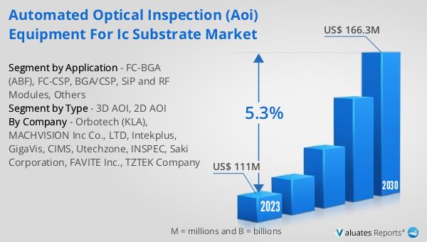
The global Automated Optical Inspection (AOI) Equipment for IC Substrate market was valued at US$ 111 million in 2023 and is anticipated to reach US$ 166.3 million by 2030, witnessing a CAGR of 5.3% during the forecast period 2024-2030. This growth is driven by the increasing demand for high-quality IC substrates in various electronic applications, including consumer electronics, automotive, telecommunications, and industrial sectors. The adoption of advanced AOI systems is essential for manufacturers to maintain high standards of quality and reliability in their products. By automating the inspection process, AOI equipment helps manufacturers achieve higher precision and efficiency, ultimately leading to better product quality and customer satisfaction. The market's growth is also supported by the continuous advancements in AOI technology, which enable more accurate and comprehensive inspection of IC substrates. As the semiconductor industry continues to evolve, the demand for AOI equipment is expected to grow, driven by the need for higher performance and reliability in electronic devices.
| Report Metric | Details |
| Report Name | Automated Optical Inspection (AOI) Equipment for IC Substrate Market |
| Accounted market size in 2023 | US$ 111 million |
| Forecasted market size in 2030 | US$ 166.3 million |
| CAGR | 5.3% |
| Base Year | 2023 |
| Forecasted years | 2024 - 2030 |
| Segment by Type |
|
| Segment by Application |
|
| Production by Region |
|
| Consumption by Region |
|
| By Company | Orbotech (KLA), MACHVISION Inc Co., LTD, Intekplus, GigaVis, CIMS, Utechzone, INSPEC, Saki Corporation, FAVITE Inc., TZTEK Company |
| Forecast units | USD million in value |
| Report coverage | Revenue and volume forecast, company share, competitive landscape, growth factors and trends |


