What is Global Wafer Bump & Pillar Inspection Equipment Market?
The Global Wafer Bump & Pillar Inspection Equipment Market is a specialized segment within the semiconductor industry that focuses on the inspection and quality control of wafer bumps and pillars. These bumps and pillars are tiny structures on semiconductor wafers that serve as connection points for electronic components. The inspection equipment used in this market ensures that these structures are correctly formed and free from defects, which is crucial for the performance and reliability of electronic devices. The market includes various types of inspection tools, such as automated optical inspection (AOI) systems, which use advanced imaging technologies to detect defects at a microscopic level. This market is essential for maintaining the high standards required in semiconductor manufacturing, as even minor defects can lead to significant performance issues in the final products. The demand for wafer bump and pillar inspection equipment is driven by the increasing complexity of semiconductor devices and the need for higher precision in manufacturing processes.
Package Substrate Bump AOI, Wafer / PLP Bump AOI in the Global Wafer Bump & Pillar Inspection Equipment Market:
Package Substrate Bump AOI and Wafer / PLP Bump AOI are two critical components of the Global Wafer Bump & Pillar Inspection Equipment Market. Package Substrate Bump AOI refers to the automated optical inspection systems used to examine the bumps on package substrates. These substrates are the base materials on which semiconductor devices are mounted, and the bumps serve as electrical connections between the device and the substrate. The AOI systems for package substrates use high-resolution cameras and advanced algorithms to detect defects such as missing bumps, misalignment, and surface irregularities. This ensures that the electrical connections are reliable and that the final product meets quality standards. On the other hand, Wafer / PLP Bump AOI focuses on inspecting the bumps on semiconductor wafers and panel-level packages (PLP). These bumps are crucial for the subsequent packaging and assembly processes. The AOI systems for wafers and PLP use similar technologies as those for package substrates but are tailored to handle the specific challenges of inspecting bumps on wafers and panels. These systems can detect a wide range of defects, including height variations, shape deformities, and contamination. The inspection process is highly automated, allowing for high throughput and consistent quality control. Both types of AOI systems play a vital role in the semiconductor manufacturing process by ensuring that the bumps are correctly formed and free from defects. This is particularly important as the industry moves towards smaller and more complex devices, where even minor defects can have significant impacts on performance and reliability. The increasing demand for advanced electronic devices, such as smartphones, tablets, and wearable technology, is driving the need for more sophisticated inspection equipment. As a result, the Global Wafer Bump & Pillar Inspection Equipment Market is expected to continue growing, with advancements in AOI technologies playing a key role in this growth.
Copper Pillar Inspection, Solder Bump Inspection in the Global Wafer Bump & Pillar Inspection Equipment Market:
The usage of Global Wafer Bump & Pillar Inspection Equipment Market in areas such as Copper Pillar Inspection and Solder Bump Inspection is crucial for maintaining the quality and reliability of semiconductor devices. Copper pillars are used in advanced packaging technologies to provide electrical connections between different layers of a semiconductor device. These pillars need to be precisely formed and free from defects to ensure proper electrical performance. Inspection equipment for copper pillars uses advanced imaging technologies to detect defects such as height variations, shape deformities, and surface contamination. This ensures that the copper pillars meet the required specifications and can perform their intended function. Solder bump inspection, on the other hand, focuses on examining the tiny solder balls used to connect semiconductor devices to substrates or other components. These solder bumps need to be accurately placed and free from defects to ensure reliable electrical connections. Inspection equipment for solder bumps uses high-resolution cameras and advanced algorithms to detect defects such as missing bumps, misalignment, and surface irregularities. This ensures that the solder bumps are correctly formed and can provide reliable electrical connections. Both copper pillar inspection and solder bump inspection are critical for the overall quality and reliability of semiconductor devices. As the industry moves towards smaller and more complex devices, the need for precise and reliable inspection equipment becomes even more important. The Global Wafer Bump & Pillar Inspection Equipment Market plays a vital role in meeting this need by providing advanced inspection solutions that ensure the quality and reliability of semiconductor devices.
Global Wafer Bump & Pillar Inspection Equipment Market Outlook:
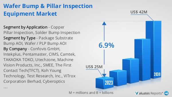
The global Wafer Bump & Pillar Inspection Equipment market was valued at US$ 25 million in 2023 and is anticipated to reach US$ 42 million by 2030, witnessing a CAGR of 6.9% during the forecast period 2024-2030. This market growth reflects the increasing demand for high-quality semiconductor devices and the need for advanced inspection equipment to ensure the reliability and performance of these devices. The market includes various types of inspection tools, such as automated optical inspection (AOI) systems, which use advanced imaging technologies to detect defects at a microscopic level. These tools are essential for maintaining the high standards required in semiconductor manufacturing, as even minor defects can lead to significant performance issues in the final products. The demand for wafer bump and pillar inspection equipment is driven by the increasing complexity of semiconductor devices and the need for higher precision in manufacturing processes. As the industry continues to evolve, the Global Wafer Bump & Pillar Inspection Equipment Market is expected to grow, with advancements in inspection technologies playing a key role in this growth.
| Report Metric | Details |
| Report Name | Wafer Bump & Pillar Inspection Equipment Market |
| Accounted market size in 2023 | US$ 25 million |
| Forecasted market size in 2030 | US$ 42 million |
| CAGR | 6.9% |
| Base Year | 2023 |
| Forecasted years | 2024 - 2030 |
| Segment by Type |
|
| Segment by Application |
|
| Production by Region |
|
| Consumption by Region |
|
| By Company | Confovis GmbH, Intekplus, Pentamaster, CIMS, Camtek, TAKAOKA TOKO, Utechzone, Machine Vision Products, Inc., SMEE, The First Contact Tech(TFCT), Koh Young Technology, Test Research, Inc., ViTrox Corporation Berhad, Cyberoptics Corporation, Omron, Mirtec, Parmi Corp, Cortex Robotics Sdn Bhd, Nordson YESTECH, PEMTRON, Hangzhou Changchuan Technology |
| Forecast units | USD million in value |
| Report coverage | Revenue and volume forecast, company share, competitive landscape, growth factors and trends |


