What is Global High Purity Yttrium Oxide (Y2O3) Power for Semiconductor Market?
The global High Purity Yttrium Oxide (Y2O3) Power for Semiconductor market is a specialized segment within the broader semiconductor industry. Yttrium Oxide, known for its high purity, is a critical material used in various semiconductor manufacturing processes. This compound is highly valued for its exceptional thermal stability, high dielectric constant, and excellent optical properties. These characteristics make it indispensable in the production of semiconductor devices, where precision and reliability are paramount. The market for High Purity Yttrium Oxide is driven by the increasing demand for advanced electronic devices, including smartphones, tablets, and other consumer electronics, as well as the growing adoption of IoT (Internet of Things) devices. As technology continues to evolve, the need for high-performance semiconductors is expected to rise, further propelling the demand for High Purity Yttrium Oxide. This market is characterized by intense competition among key players, continuous innovation, and a focus on maintaining the highest standards of purity and quality.
Agglomerated, Agglomerated and Sintered in the Global High Purity Yttrium Oxide (Y2O3) Power for Semiconductor Market:
In the context of the Global High Purity Yttrium Oxide (Y2O3) Power for Semiconductor Market, the terms "Agglomerated" and "Agglomerated and Sintered" refer to specific forms and processes of the material that impact its performance and application. Agglomerated Yttrium Oxide refers to particles that have been clustered together to form larger, more manageable granules. This process is essential for improving the flowability and handling of the powder, making it easier to use in various semiconductor manufacturing processes. Agglomeration helps in reducing dust generation, which is crucial in maintaining a clean and controlled environment in semiconductor fabrication facilities. On the other hand, Agglomerated and Sintered Yttrium Oxide involves an additional step where the agglomerated particles are subjected to high temperatures to fuse them together. This sintering process enhances the mechanical strength and structural integrity of the material, making it more suitable for applications that require high durability and resistance to thermal and mechanical stresses. The sintered form of Yttrium Oxide is particularly beneficial in processes like Chemical Vapor Deposition (CVD) and Physical Vapor Deposition (PVD), where the material needs to withstand high temperatures and aggressive chemical environments. The choice between agglomerated and agglomerated and sintered forms depends on the specific requirements of the semiconductor manufacturing process. For instance, in applications where high precision and minimal contamination are critical, the sintered form may be preferred due to its superior structural properties. Conversely, for processes that prioritize ease of handling and cost-effectiveness, the agglomerated form might be more suitable. Both forms play a vital role in ensuring the efficiency and reliability of semiconductor manufacturing, contributing to the overall performance and quality of the final electronic devices. The continuous advancements in semiconductor technology and the increasing complexity of electronic devices necessitate the use of high-quality materials like High Purity Yttrium Oxide. As such, understanding the differences between agglomerated and agglomerated and sintered forms is crucial for manufacturers to make informed decisions and optimize their production processes.
Semiconductor Etch Equipment, Deposition (CVD, PVD, ALD), Ion Implant Equipment, Others in the Global High Purity Yttrium Oxide (Y2O3) Power for Semiconductor Market:
The usage of Global High Purity Yttrium Oxide (Y2O3) Power in the semiconductor market spans several critical areas, including Semiconductor Etch Equipment, Deposition (CVD, PVD, ALD), Ion Implant Equipment, and others. In Semiconductor Etch Equipment, High Purity Yttrium Oxide is used as a protective coating material due to its excellent resistance to plasma and chemical etching processes. This ensures the longevity and reliability of the etching equipment, which is essential for creating precise patterns on semiconductor wafers. The high purity of Yttrium Oxide minimizes the risk of contamination, which is crucial for maintaining the integrity of the semiconductor devices. In Deposition processes such as Chemical Vapor Deposition (CVD), Physical Vapor Deposition (PVD), and Atomic Layer Deposition (ALD), High Purity Yttrium Oxide serves as a critical material for creating thin films and coatings. These processes require materials that can withstand high temperatures and aggressive chemical environments, and Yttrium Oxide's thermal stability and chemical resistance make it an ideal choice. The high dielectric constant of Yttrium Oxide also makes it valuable in the production of high-k dielectric materials, which are essential for advanced semiconductor devices. In Ion Implant Equipment, High Purity Yttrium Oxide is used as a coating material to protect the equipment from the harsh conditions of the ion implantation process. This process involves bombarding the semiconductor wafer with ions to alter its electrical properties, and the equipment used must be able to withstand the high-energy ions and reactive gases involved. Yttrium Oxide's durability and resistance to ion bombardment make it an excellent choice for this application. Beyond these specific areas, High Purity Yttrium Oxide is also used in other semiconductor manufacturing processes where high purity, thermal stability, and chemical resistance are required. This includes applications in lithography, where it can be used as a coating material for photomasks and other components, and in packaging, where it can be used to protect sensitive electronic components from environmental factors. The versatility and high performance of High Purity Yttrium Oxide make it an indispensable material in the semiconductor industry, contributing to the production of reliable and high-performance electronic devices.
Global High Purity Yttrium Oxide (Y2O3) Power for Semiconductor Market Outlook:
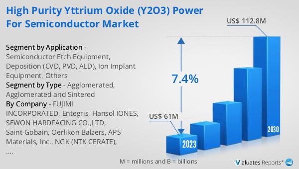
The global High Purity Yttrium Oxide (Y2O3) Power for Semiconductor market was valued at US$ 61 million in 2023 and is anticipated to reach US$ 112.8 million by 2030, witnessing a CAGR of 7.4% during the forecast period 2024-2030. According to SEMI, worldwide sales of semiconductor manufacturing equipment increased by 5% from $102.6 billion in 2021 to an all-time record of $107.6 billion in 2022. For the third consecutive year, China remained the largest semiconductor equipment market in 2022, despite a 5% slowdown in the pace of investments in the region year over year, accounting for $28.3 billion in billings. This growth in the semiconductor equipment market underscores the increasing demand for advanced materials like High Purity Yttrium Oxide, which are essential for the production of high-performance semiconductor devices. The continuous advancements in semiconductor technology and the growing complexity of electronic devices are driving the need for materials that can meet the stringent requirements of modern manufacturing processes. High Purity Yttrium Oxide, with its exceptional thermal stability, high dielectric constant, and excellent optical properties, is well-positioned to meet these demands and support the ongoing growth of the semiconductor industry.
| Report Metric | Details |
| Report Name | High Purity Yttrium Oxide (Y2O3) Power for Semiconductor Market |
| Accounted market size in 2023 | US$ 61 million |
| Forecasted market size in 2030 | US$ 112.8 million |
| CAGR | 7.4% |
| Base Year | 2023 |
| Forecasted years | 2024 - 2030 |
| Segment by Type |
|
| Segment by Application |
|
| Production by Region |
|
| Consumption by Region |
|
| By Company | FUJIMI INCORPORATED, Entegris, Hansol IONES, SEWON HARDFACING CO.,LTD, Saint-Gobain, Oerlikon Balzers, APS Materials, Inc., NGK (NTK CERATE), FEMVIX CORP., CINOS, Yeedex, YMC Co., Ltd., Treibacher Industrie AG, Nano Research Elements, Coorstek, Shin-Etsu Rare Earths |
| Forecast units | USD million in value |
| Report coverage | Revenue and volume forecast, company share, competitive landscape, growth factors and trends |


