What is Global Metal Chambers for Semiconductor Equipment Market?
The global Metal Chambers for Semiconductor Equipment market is a specialized segment within the semiconductor industry that focuses on the production and utilization of metal chambers used in various semiconductor manufacturing processes. These chambers are essential components in the fabrication of semiconductor devices, providing controlled environments for processes such as deposition, etching, and lithography. The market for these metal chambers is driven by the increasing demand for advanced semiconductor devices, which are integral to a wide range of electronic products, from smartphones to automotive systems. As technology advances, the need for more precise and efficient semiconductor manufacturing equipment grows, leading to a corresponding increase in the demand for high-quality metal chambers. These chambers are designed to withstand extreme conditions, such as high temperatures and corrosive environments, ensuring the reliability and performance of the semiconductor manufacturing process. The market is characterized by continuous innovation and development, with manufacturers striving to improve the durability, efficiency, and functionality of their products to meet the evolving needs of the semiconductor industry.
Reaction Chamber, Transfer Chamber, Load Lock Chamber in the Global Metal Chambers for Semiconductor Equipment Market:
In the context of the Global Metal Chambers for Semiconductor Equipment Market, various types of chambers play crucial roles in the semiconductor manufacturing process. The Reaction Chamber is one of the most critical components, used primarily in chemical vapor deposition (CVD) and physical vapor deposition (PVD) processes. These chambers provide a controlled environment where chemical reactions occur, allowing for the precise deposition of thin films on semiconductor wafers. The materials used in reaction chambers must be highly resistant to corrosion and capable of withstanding high temperatures to ensure the integrity of the deposition process. Transfer Chambers, on the other hand, are used to move semiconductor wafers between different processing stations within a fabrication facility. These chambers are designed to maintain a clean and controlled environment to prevent contamination of the wafers during transfer. Load Lock Chambers serve as an interface between the external environment and the vacuum environment of the processing chambers. They allow for the introduction and removal of wafers without compromising the vacuum conditions necessary for various semiconductor manufacturing processes. Load lock chambers are essential for maintaining the efficiency and cleanliness of the fabrication process, as they minimize the exposure of wafers to potential contaminants. Each of these chambers plays a vital role in ensuring the precision, efficiency, and reliability of semiconductor manufacturing, contributing to the overall performance and quality of the final semiconductor devices.
Deposition (CVD, PVD, AlD), Etching Equipment, E-beam and Lithography, Implant, Others in the Global Metal Chambers for Semiconductor Equipment Market:
The usage of Global Metal Chambers for Semiconductor Equipment Market spans several critical areas in semiconductor manufacturing, including Deposition (CVD, PVD, ALD), Etching Equipment, E-beam and Lithography, Implant, and others. In deposition processes such as Chemical Vapor Deposition (CVD), Physical Vapor Deposition (PVD), and Atomic Layer Deposition (ALD), metal chambers provide the controlled environments necessary for the precise application of thin films on semiconductor wafers. These films are essential for creating the various layers and structures within semiconductor devices. The chambers must be designed to handle the specific chemical reactions and physical conditions required for each deposition method, ensuring uniformity and quality of the deposited materials. In etching equipment, metal chambers are used to create the precise patterns and structures on semiconductor wafers by selectively removing material. The chambers must maintain a stable environment to ensure the accuracy and consistency of the etching process, which is critical for the performance of the final semiconductor devices. E-beam and lithography processes also rely on metal chambers to provide the controlled environments necessary for the precise patterning of semiconductor wafers. These processes involve the use of electron beams or light to create intricate patterns on the wafers, and the chambers must be designed to minimize contamination and ensure the accuracy of the patterning. In implant processes, metal chambers are used to introduce dopants into semiconductor wafers, altering their electrical properties to create the desired semiconductor characteristics. The chambers must be capable of maintaining the precise conditions necessary for the implantation process, ensuring the uniformity and quality of the doped regions. Overall, the usage of metal chambers in these various areas of semiconductor manufacturing is essential for ensuring the precision, efficiency, and reliability of the processes, contributing to the overall performance and quality of the final semiconductor devices.
Global Metal Chambers for Semiconductor Equipment Market Outlook:
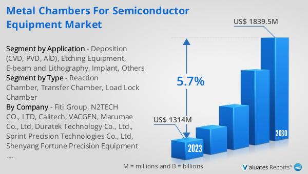
The global Metal Chambers for Semiconductor Equipment market was valued at US$ 1314 million in 2023 and is anticipated to reach US$ 1839.5 million by 2030, witnessing a CAGR of 5.7% during the forecast period 2024-2030. According to SEMI, worldwide sales of semiconductor manufacturing equipment increased 5% from $102.6 billion in 2021 to an all-time record of $107.6 billion in 2022. For the third consecutive year, China remained the largest semiconductor equipment market in 2022, despite a 5% slowdown in the pace of investments in the region year over year, accounting for $28.3 billion in billings. This growth in the semiconductor equipment market highlights the increasing demand for advanced semiconductor devices and the corresponding need for high-quality metal chambers to support the manufacturing processes. The continuous innovation and development in the semiconductor industry drive the demand for more precise and efficient manufacturing equipment, including metal chambers, which are essential for maintaining the controlled environments necessary for various semiconductor fabrication processes. The market outlook indicates a positive trend, with significant growth expected in the coming years, driven by the ongoing advancements in semiconductor technology and the increasing demand for electronic devices across various industries.
| Report Metric | Details |
| Report Name | Metal Chambers for Semiconductor Equipment Market |
| Accounted market size in 2023 | US$ 1314 million |
| Forecasted market size in 2030 | US$ 1839.5 million |
| CAGR | 5.7% |
| Base Year | 2023 |
| Forecasted years | 2024 - 2030 |
| Segment by Type |
|
| Segment by Application |
|
| Production by Region |
|
| Consumption by Region |
|
| By Company | Fiti Group, N2TECH CO., LTD, Calitech, VACGEN, Marumae Co., Ltd, Duratek Technology Co., Ltd., Sprint Precision Technologies Co., Ltd, Shenyang Fortune Precision Equipment Co., Ltd, Tolerance, Sanyue Semiconductor Technology, BoBoo |
| Forecast units | USD million in value |
| Report coverage | Revenue and volume forecast, company share, competitive landscape, growth factors and trends |


