What is Global Photomask Lithography Equipment Market?
The Global Photomask Lithography Equipment Market is a specialized segment within the broader semiconductor and electronics manufacturing industry. Photomask lithography equipment is essential for the production of photomasks, which are used to transfer circuit patterns onto semiconductor wafers. These photomasks are critical in the fabrication of integrated circuits (ICs), displays, and other electronic components. The market encompasses various types of lithography equipment, including direct write lithography (DLW) and electron beam lithography (EBL) systems. These technologies enable the precise patterning required for advanced semiconductor devices and high-resolution displays. The demand for photomask lithography equipment is driven by the continuous advancements in semiconductor technology, the increasing complexity of IC designs, and the growing need for high-performance electronic devices. As the industry evolves, the market for photomask lithography equipment is expected to expand, driven by innovations in lithography techniques and the rising demand for miniaturized and efficient electronic components.
Direct Write Lithography (DLW), Electron Beam Lithography System (EBL) in the Global Photomask Lithography Equipment Market:
Direct Write Lithography (DLW) and Electron Beam Lithography (EBL) are two advanced technologies within the Global Photomask Lithography Equipment Market. DLW is a maskless lithography technique that directly writes patterns onto a substrate using a focused beam of light or electrons. This method offers high flexibility and precision, making it suitable for prototyping and small-scale production. DLW is particularly advantageous for applications requiring rapid design changes and customization, as it eliminates the need for photomasks. On the other hand, Electron Beam Lithography (EBL) uses a focused beam of electrons to create extremely fine patterns on a substrate. EBL is known for its high resolution and accuracy, making it ideal for fabricating nanoscale structures and advanced semiconductor devices. EBL systems are widely used in research and development, as well as in the production of photomasks for cutting-edge semiconductor manufacturing. Both DLW and EBL play crucial roles in the photomask lithography equipment market, catering to the diverse needs of the semiconductor and electronics industries. These technologies enable the production of intricate and high-precision patterns, supporting the development of next-generation electronic devices and components. As the demand for smaller, faster, and more efficient electronic devices continues to grow, the importance of DLW and EBL in the photomask lithography equipment market is expected to increase, driving further advancements in lithography techniques and equipment.
Semiconductor/IC, Display/LCD, OLED/PCB, Others in the Global Photomask Lithography Equipment Market:
The usage of Global Photomask Lithography Equipment Market spans several key areas, including Semiconductor/IC, Display/LCD, OLED/PCB, and others. In the semiconductor industry, photomask lithography equipment is essential for the fabrication of integrated circuits (ICs). Photomasks are used to transfer intricate circuit patterns onto semiconductor wafers, enabling the production of high-performance ICs used in various electronic devices, such as smartphones, computers, and automotive electronics. The precision and accuracy of photomask lithography equipment are critical for achieving the miniaturization and complexity required in modern IC designs. In the display industry, photomask lithography equipment is used to produce high-resolution displays, including LCDs and OLEDs. Photomasks are employed to pattern the thin-film transistors (TFTs) and other components that make up the display panels. The demand for high-definition and energy-efficient displays drives the need for advanced photomask lithography equipment capable of producing fine and accurate patterns. In the PCB (Printed Circuit Board) industry, photomask lithography equipment is used to create the intricate circuitry on PCBs, which are essential for connecting and supporting electronic components in various devices. The precision of photomask lithography ensures the reliability and performance of PCBs in applications ranging from consumer electronics to industrial equipment. Additionally, photomask lithography equipment finds applications in other areas, such as MEMS (Micro-Electro-Mechanical Systems), photonics, and nanotechnology. These applications require high-precision patterning to create microscale and nanoscale structures with specific functionalities. Overall, the Global Photomask Lithography Equipment Market plays a vital role in enabling the production of advanced electronic devices and components across various industries, supporting technological innovation and development.
Global Photomask Lithography Equipment Market Outlook:
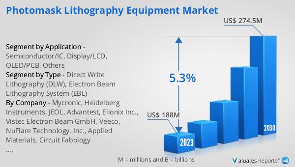
The global Photomask Lithography Equipment market was valued at US$ 188 million in 2023 and is anticipated to reach US$ 274.5 million by 2030, witnessing a CAGR of 5.3% during the forecast period 2024-2030. This growth reflects the increasing demand for advanced lithography equipment driven by the continuous advancements in semiconductor technology and the growing complexity of integrated circuit designs. The market's expansion is also fueled by the rising need for high-performance electronic devices, which require precise and accurate patterning capabilities. As the semiconductor and electronics industries continue to evolve, the demand for photomask lithography equipment is expected to grow, supporting the development of next-generation electronic components and devices. The market outlook indicates a positive trend, with significant opportunities for innovation and growth in the coming years.
| Report Metric | Details |
| Report Name | Photomask Lithography Equipment Market |
| Accounted market size in 2023 | US$ 188 million |
| Forecasted market size in 2030 | US$ 274.5 million |
| CAGR | 5.3% |
| Base Year | 2023 |
| Forecasted years | 2024 - 2030 |
| Segment by Type |
|
| Segment by Application |
|
| Production by Region |
|
| Consumption by Region |
|
| By Company | Mycronic, Heidelberg Instruments, JEOL, Advantest, Elionix Inc., Vistec Electron Beam GmbH, Veeco, NuFlare Technology, Inc., Applied Materials, Circuit Fabology Microelectronics Equipment Co.,Ltd., Jiangsu Yingsu IC Equipment |
| Forecast units | USD million in value |
| Report coverage | Revenue and volume forecast, company share, competitive landscape, growth factors and trends |


