What is Global Laser Direct Imaging (LDI) System for Advanced Packaging Market?
Global Laser Direct Imaging (LDI) System for Advanced Packaging Market is a specialized technology used in the semiconductor industry to create intricate patterns on substrates, which are essential for advanced packaging solutions. This system employs laser technology to directly image the desired patterns onto the substrate, eliminating the need for traditional photomasks. This not only enhances precision but also significantly reduces production time and costs. The LDI system is particularly crucial for advanced packaging techniques such as fan-out wafer-level packaging (FOWLP), flip-chip, and 3D integrated circuits (3D ICs). These techniques are essential for producing smaller, faster, and more efficient electronic devices. The global market for LDI systems is driven by the increasing demand for miniaturized electronic devices, advancements in semiconductor technology, and the need for high-performance computing solutions. As the electronics industry continues to evolve, the adoption of LDI systems is expected to grow, making it a vital component in the future of semiconductor manufacturing.
FC (FCCSP, FCBGA), WLCSP in the Global Laser Direct Imaging (LDI) System for Advanced Packaging Market:
FC (Flip-Chip), FCCSP (Flip-Chip Chip Scale Package), and FCBGA (Flip-Chip Ball Grid Array) are advanced packaging technologies that benefit significantly from Global Laser Direct Imaging (LDI) Systems. Flip-Chip technology involves mounting the semiconductor chip upside down on the substrate, allowing for a direct electrical connection through solder bumps. This method enhances electrical performance and heat dissipation, making it ideal for high-performance applications. FCCSP is a variation of Flip-Chip technology where the chip is mounted on a smaller substrate, resulting in a compact package that is suitable for mobile devices and other space-constrained applications. FCBGA, on the other hand, uses an array of solder balls to connect the chip to the substrate, providing a robust and reliable connection for high-density and high-performance applications. LDI systems play a crucial role in these technologies by enabling precise patterning of the substrate, which is essential for the accurate placement of solder bumps and balls. This precision ensures optimal electrical performance and reliability of the final product. WLCSP (Wafer-Level Chip Scale Package) is another advanced packaging technology that benefits from LDI systems. In WLCSP, the entire semiconductor wafer is processed and tested before being diced into individual chips. This method reduces manufacturing costs and improves yield by allowing for the simultaneous processing of multiple chips. LDI systems are used to create the intricate patterns on the wafer that are necessary for the electrical connections and protective layers. The high precision and accuracy of LDI systems ensure that the patterns are correctly aligned, which is critical for the performance and reliability of the final product. Overall, the use of LDI systems in FC, FCCSP, FCBGA, and WLCSP technologies enhances the performance, reliability, and cost-effectiveness of advanced packaging solutions, making them essential for the production of modern electronic devices.
300mm Wafer, 200mm Wafer in the Global Laser Direct Imaging (LDI) System for Advanced Packaging Market:
The usage of Global Laser Direct Imaging (LDI) Systems in the context of 300mm and 200mm wafers is pivotal for the semiconductor industry, particularly in advanced packaging applications. A 300mm wafer, being larger in diameter compared to a 200mm wafer, allows for the production of more semiconductor devices per wafer, thereby increasing manufacturing efficiency and reducing costs. LDI systems are crucial in this process as they provide the precision needed to create intricate patterns on these larger wafers. The high-resolution imaging capabilities of LDI systems ensure that even the smallest features are accurately reproduced, which is essential for the performance and reliability of the final semiconductor devices. For 300mm wafers, LDI systems enable the production of advanced packaging solutions such as fan-out wafer-level packaging (FOWLP) and 3D integrated circuits (3D ICs). These packaging techniques require precise patterning to ensure proper alignment and connectivity of the various components. The use of LDI systems in this context not only enhances the performance of the final product but also reduces production time and costs. On the other hand, 200mm wafers, while smaller in diameter, are still widely used in the semiconductor industry, particularly for applications that do not require the high volume production capabilities of 300mm wafers. LDI systems are equally important for 200mm wafers as they provide the same level of precision and accuracy needed for advanced packaging solutions. The ability to create intricate patterns on these smaller wafers ensures that the final semiconductor devices meet the required performance and reliability standards. Additionally, the use of LDI systems in 200mm wafer processing allows for the production of a wide range of semiconductor devices, from simple integrated circuits to complex system-on-chips (SoCs). This versatility makes LDI systems an essential tool for semiconductor manufacturers, regardless of the wafer size. In summary, the usage of Global Laser Direct Imaging (LDI) Systems in both 300mm and 200mm wafer processing is critical for the production of advanced packaging solutions. The precision and accuracy provided by LDI systems ensure that the final semiconductor devices meet the highest performance and reliability standards, making them indispensable for the semiconductor industry.
Global Laser Direct Imaging (LDI) System for Advanced Packaging Market Outlook:
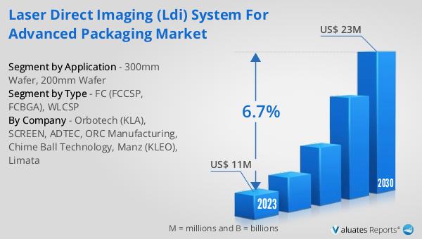
The global market for Laser Direct Imaging (LDI) Systems for Advanced Packaging was valued at approximately $11 million in 2023 and is projected to reach around $23 million by 2030, reflecting a compound annual growth rate (CAGR) of 6.7% during the forecast period from 2024 to 2030. This growth is driven by the increasing demand for miniaturized electronic devices, advancements in semiconductor technology, and the need for high-performance computing solutions. As the electronics industry continues to evolve, the adoption of LDI systems is expected to grow, making it a vital component in the future of semiconductor manufacturing. The precision and efficiency offered by LDI systems make them indispensable for advanced packaging solutions, which are essential for producing smaller, faster, and more efficient electronic devices. The market outlook indicates a positive trend, with significant growth opportunities for LDI system manufacturers and suppliers in the coming years.
| Report Metric | Details |
| Report Name | Laser Direct Imaging (LDI) System for Advanced Packaging Market |
| Accounted market size in 2023 | US$ 11 million |
| Forecasted market size in 2030 | US$ 23 million |
| CAGR | 6.7% |
| Base Year | 2023 |
| Forecasted years | 2024 - 2030 |
| Segment by Type |
|
| Segment by Application |
|
| Production by Region |
|
| Consumption by Region |
|
| By Company | Orbotech (KLA), SCREEN, ADTEC, ORC Manufacturing, Chime Ball Technology, Manz (KLEO), Limata |
| Forecast units | USD million in value |
| Report coverage | Revenue and volume forecast, company share, competitive landscape, growth factors and trends |


