What is Global AOI (Automated Optical Inspection) for Advanced Packaging Market?
Global AOI (Automated Optical Inspection) for Advanced Packaging Market is a specialized segment within the broader electronics manufacturing industry. This market focuses on the use of automated optical inspection systems to ensure the quality and reliability of advanced packaging technologies. Advanced packaging refers to the methods used to interconnect semiconductor devices, such as wafer-level packaging (WLP), panel-level packaging (PLP), and flip-chip (FC) technologies. These methods are crucial for producing smaller, faster, and more efficient electronic devices. AOI systems play a vital role in this process by using cameras and imaging software to detect defects and ensure that each component meets stringent quality standards. The global AOI market for advanced packaging is driven by the increasing demand for high-performance electronic devices, the need for miniaturization, and the growing complexity of semiconductor manufacturing processes. As technology continues to evolve, the importance of AOI systems in maintaining the integrity and performance of advanced packaging solutions is expected to grow, making it a critical component of the semiconductor manufacturing ecosystem.
3D AOI system, 2D AOI system in the Global AOI (Automated Optical Inspection) for Advanced Packaging Market:
3D AOI systems and 2D AOI systems are two primary types of automated optical inspection technologies used in the global AOI market for advanced packaging. 3D AOI systems utilize multiple cameras and advanced imaging techniques to create a three-dimensional representation of the inspected object. This allows for a more comprehensive analysis of the component, including height, volume, and surface characteristics. 3D AOI systems are particularly effective in detecting complex defects such as solder joint issues, component misalignment, and warpage, which are critical in advanced packaging applications. On the other hand, 2D AOI systems rely on high-resolution cameras to capture two-dimensional images of the inspected object. These systems are typically used for simpler inspections, such as checking for missing components, incorrect placements, and surface defects. While 2D AOI systems are generally faster and less expensive than their 3D counterparts, they may not be as effective in detecting certain types of defects that require depth information. In the context of advanced packaging, both 3D and 2D AOI systems play complementary roles. 3D AOI systems are often used in the early stages of the manufacturing process, where precise measurements and defect detection are crucial. 2D AOI systems, on the other hand, are commonly employed in later stages for final inspections and quality control. The choice between 3D and 2D AOI systems depends on various factors, including the complexity of the packaging technology, the specific inspection requirements, and the cost considerations. As the demand for advanced packaging solutions continues to rise, the integration of both 3D and 2D AOI systems is expected to become increasingly important in ensuring the quality and reliability of semiconductor devices.
WLP (wafer-leve-packaging), PLP (panel-level-packaging), FC (FCCSP, FC BGA) in the Global AOI (Automated Optical Inspection) for Advanced Packaging Market:
The usage of Global AOI (Automated Optical Inspection) for Advanced Packaging Market in areas such as wafer-level packaging (WLP), panel-level packaging (PLP), and flip-chip (FC) technologies is crucial for maintaining high standards of quality and reliability. In wafer-level packaging (WLP), AOI systems are used to inspect the entire wafer before it is diced into individual chips. This ensures that any defects are identified and addressed early in the manufacturing process, reducing the risk of defective chips reaching the final product. AOI systems in WLP applications are particularly effective in detecting issues such as die cracks, surface contamination, and alignment errors. In panel-level packaging (PLP), AOI systems are used to inspect large panels that contain multiple semiconductor devices. This approach allows for higher throughput and cost efficiency compared to traditional wafer-level packaging. AOI systems in PLP applications are designed to handle the larger inspection area and are equipped with advanced imaging technologies to detect defects such as delamination, voids, and misalignment. In flip-chip (FC) technologies, which include FCCSP (flip-chip chip-scale package) and FC BGA (flip-chip ball grid array), AOI systems are used to inspect the solder bumps and interconnects that connect the chip to the substrate. These inspections are critical for ensuring the reliability and performance of the final product, as defects in the solder joints can lead to electrical failures and reduced device lifespan. AOI systems in FC applications are capable of detecting issues such as solder voids, bridging, and insufficient solder volume. Overall, the integration of AOI systems in WLP, PLP, and FC technologies is essential for achieving high yields, reducing manufacturing costs, and ensuring the production of high-quality semiconductor devices.
Global AOI (Automated Optical Inspection) for Advanced Packaging Market Outlook:
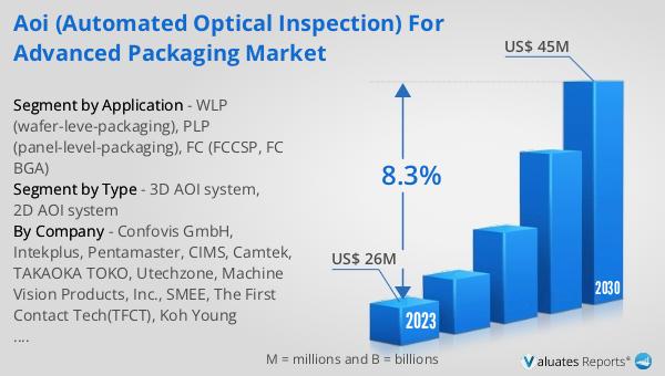
The global AOI (Automated Optical Inspection) for Advanced Packaging market was valued at US$ 26 million in 2023 and is anticipated to reach US$ 45 million by 2030, witnessing a CAGR of 8.3% during the forecast period from 2024 to 2030. This growth is driven by the increasing demand for high-performance electronic devices, the need for miniaturization, and the growing complexity of semiconductor manufacturing processes. As technology continues to evolve, the importance of AOI systems in maintaining the integrity and performance of advanced packaging solutions is expected to grow. The market outlook for AOI systems in advanced packaging is positive, with significant opportunities for growth and innovation. The adoption of AOI systems is expected to increase as manufacturers seek to improve yield rates, reduce production costs, and ensure the quality and reliability of their products. The integration of advanced imaging technologies, such as 3D AOI systems, is likely to play a key role in addressing the challenges associated with advanced packaging technologies. Overall, the global AOI market for advanced packaging is poised for significant growth, driven by the ongoing advancements in semiconductor manufacturing and the increasing demand for high-quality electronic devices.
| Report Metric | Details |
| Report Name | AOI (Automated Optical Inspection) for Advanced Packaging Market |
| Accounted market size in 2023 | US$ 26 million |
| Forecasted market size in 2030 | US$ 45 million |
| CAGR | 8.3% |
| Base Year | 2023 |
| Forecasted years | 2024 - 2030 |
| Segment by Type |
|
| Segment by Application |
|
| Production by Region |
|
| Consumption by Region |
|
| By Company | Confovis GmbH, Intekplus, Pentamaster, CIMS, Camtek, TAKAOKA TOKO, Utechzone, Machine Vision Products, Inc., SMEE, The First Contact Tech(TFCT), Koh Young Technology, Test Research, Inc., ViTrox Corporation Berhad, Cyberoptics Corporation, Omron, Mirtec, Parmi Corp, Cortex Robotics Sdn Bhd, Nordson YESTECH, Hangzhou Changchuan Technology |
| Forecast units | USD million in value |
| Report coverage | Revenue and volume forecast, company share, competitive landscape, growth factors and trends |


