What is Global Photomask Manufacturing and Inspection Equipment Market?
The Global Photomask Manufacturing and Inspection Equipment Market is a specialized sector within the broader semiconductor and electronics industry. Photomasks are essential tools used in the photolithography process to transfer circuit patterns onto semiconductor wafers, which are then used to manufacture integrated circuits (ICs), displays, and other electronic components. The market for photomask manufacturing and inspection equipment includes various types of machinery and tools designed to create, clean, etch, and inspect these photomasks to ensure they meet the high precision and quality standards required in the industry. This market is driven by the increasing demand for advanced electronic devices, the miniaturization of semiconductor components, and the need for high-resolution displays. As technology continues to evolve, the photomask manufacturing and inspection equipment market is expected to grow, driven by innovations in semiconductor fabrication and the rising adoption of advanced manufacturing techniques.
Direct Write Lithography (DLW), Electron Beam Lithography System (EBL), Photomask Cleaning Equipment, Photomask Etching Equipment, Photomask Inspection System in the Global Photomask Manufacturing and Inspection Equipment Market:
Direct Write Lithography (DLW) is a technique used in the photomask manufacturing process that allows for the direct writing of patterns onto a substrate without the need for a photomask. This method is highly precise and is often used for creating complex and intricate designs that are difficult to achieve with traditional photolithography. Electron Beam Lithography System (EBL) is another advanced technique that uses a focused beam of electrons to draw custom patterns on a surface covered with an electron-sensitive film. EBL is known for its high resolution and is commonly used in research and development for creating nanoscale devices. Photomask Cleaning Equipment is essential for maintaining the quality and longevity of photomasks. These machines use various cleaning methods, such as ultrasonic cleaning, to remove contaminants and particles from the photomask surface, ensuring that the patterns are transferred accurately during the photolithography process. Photomask Etching Equipment is used to etch the desired patterns onto the photomask substrate. This equipment uses chemical or plasma etching techniques to create precise and intricate designs on the photomask, which are then used to transfer these patterns onto semiconductor wafers. Photomask Inspection Systems are critical for ensuring the quality and accuracy of photomasks. These systems use advanced imaging and analysis techniques to detect defects and irregularities in the photomask patterns, ensuring that only high-quality photomasks are used in the semiconductor manufacturing process. The combination of these advanced technologies and equipment ensures that the photomask manufacturing process is efficient, precise, and capable of meeting the high standards required in the semiconductor industry.
Semiconductor/IC Photomask, Display/LCD Photomask, OLED/PCB Photomask, Others in the Global Photomask Manufacturing and Inspection Equipment Market:
The Global Photomask Manufacturing and Inspection Equipment Market plays a crucial role in various areas, including Semiconductor/IC Photomask, Display/LCD Photomask, OLED/PCB Photomask, and others. In the semiconductor industry, photomasks are used to transfer intricate circuit patterns onto silicon wafers, which are then processed to create integrated circuits (ICs). The precision and accuracy of photomasks are critical in ensuring the performance and reliability of ICs, making photomask manufacturing and inspection equipment essential in this sector. In the display industry, photomasks are used to create patterns for LCD and OLED displays. These displays require high-resolution and high-precision photomasks to ensure the quality and clarity of the final product. Photomask manufacturing and inspection equipment are used to create and inspect these photomasks, ensuring that they meet the stringent requirements of the display industry. In the PCB (Printed Circuit Board) industry, photomasks are used to transfer circuit patterns onto the PCB substrate. The accuracy and precision of these patterns are critical in ensuring the performance and reliability of the final PCB. Photomask manufacturing and inspection equipment are used to create and inspect these photomasks, ensuring that they meet the high standards required in the PCB industry. Other areas where photomask manufacturing and inspection equipment are used include the production of MEMS (Micro-Electro-Mechanical Systems), sensors, and other advanced electronic components. The precision and accuracy of photomasks are critical in these areas, making photomask manufacturing and inspection equipment essential in ensuring the quality and performance of the final products. Overall, the Global Photomask Manufacturing and Inspection Equipment Market plays a vital role in various industries, ensuring the quality and performance of a wide range of electronic components and devices.
Global Photomask Manufacturing and Inspection Equipment Market Outlook:
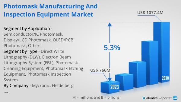
The global Photomask Manufacturing and Inspection Equipment market was valued at US$ 766 million in 2023 and is anticipated to reach US$ 1077.4 million by 2030, witnessing a CAGR of 5.3% during the forecast period 2024-2030. This growth is driven by the increasing demand for advanced electronic devices, the miniaturization of semiconductor components, and the need for high-resolution displays. As technology continues to evolve, the photomask manufacturing and inspection equipment market is expected to grow, driven by innovations in semiconductor fabrication and the rising adoption of advanced manufacturing techniques. The market outlook indicates a positive trend, with significant growth opportunities in various sectors, including semiconductor, display, and PCB industries. The increasing complexity and precision required in these industries are driving the demand for advanced photomask manufacturing and inspection equipment, ensuring the quality and performance of the final products. Overall, the market outlook for the Global Photomask Manufacturing and Inspection Equipment Market is promising, with significant growth potential in the coming years.
| Report Metric | Details |
| Report Name | Photomask Manufacturing and Inspection Equipment Market |
| Accounted market size in 2023 | US$ 766 million |
| Forecasted market size in 2030 | US$ 1077.4 million |
| CAGR | 5.3% |
| Base Year | 2023 |
| Forecasted years | 2024 - 2030 |
| Segment by Type |
|
| Segment by Application |
|
| By Region |
|
| By Company | Mycronic, Heidelberg Instruments, JEOL, Advantest, Elionix Inc., Vistec Electron Beam GmbH, Veeco, NuFlare Technology, Inc., SÜSS MicroTec SE, Orbotech (KLA), SHIBAURA MECHATRONICS, V-Technology, ZEISS Group, Lasertec Corporation, SINTO S-PRECISION, ASML(HMI), Applied Materials, Technovision, Amaya CO., LTD, Micro Engineering Inc, Ulvac, Circuit Fabology Microelectronics Equipment Co.,Ltd., Jiangsu Yingsu IC Equipment, Beijing Hualin Jiaye |
| Forecast units | USD million in value |
| Report coverage | Revenue and volume forecast, company share, competitive landscape, growth factors and trends |


