What is Global Automated Optical Inspection (AOI) Equipment for Semiconductor Market?
Global Automated Optical Inspection (AOI) Equipment for Semiconductor Market refers to the advanced technology used to inspect semiconductor devices for defects during the manufacturing process. This equipment uses optical systems to capture high-resolution images of semiconductor wafers and components, which are then analyzed by sophisticated software to detect any anomalies or defects. The primary goal of AOI equipment is to ensure the quality and reliability of semiconductor products by identifying defects early in the production process, thereby reducing the risk of faulty products reaching the market. This technology is crucial for maintaining the high standards required in the semiconductor industry, where even minor defects can lead to significant performance issues. The global market for AOI equipment is driven by the increasing demand for high-quality semiconductors in various applications, including consumer electronics, automotive, telecommunications, and industrial sectors. As the complexity of semiconductor devices continues to grow, the need for more advanced inspection solutions becomes increasingly important.
2D AOI Inspection System for Semiconductor, 3D AOI Inspection System for Semiconductor in the Global Automated Optical Inspection (AOI) Equipment for Semiconductor Market:
2D AOI Inspection Systems for semiconductors are designed to inspect the surface of semiconductor wafers and components using two-dimensional imaging technology. These systems capture high-resolution images of the wafer surface and analyze them to detect defects such as scratches, contamination, and pattern deviations. The primary advantage of 2D AOI systems is their ability to quickly and accurately identify surface-level defects, making them ideal for applications where surface quality is critical. However, 2D AOI systems have limitations when it comes to detecting defects that are not visible on the surface, such as those that occur within the layers of the semiconductor device. On the other hand, 3D AOI Inspection Systems offer a more comprehensive inspection solution by capturing three-dimensional images of semiconductor wafers and components. These systems use advanced imaging techniques, such as laser triangulation and structured light, to create detailed 3D models of the inspected objects. This allows for the detection of both surface and subsurface defects, providing a more thorough inspection process. 3D AOI systems are particularly useful for inspecting complex semiconductor devices with multiple layers, such as advanced packaging and MEMS (Micro-Electro-Mechanical Systems). The ability to detect defects at different depths within the device makes 3D AOI systems an essential tool for ensuring the quality and reliability of modern semiconductor products. In the context of the global AOI equipment market, both 2D and 3D AOI systems play a crucial role in meeting the diverse inspection needs of the semiconductor industry. As the demand for more advanced and reliable semiconductor devices continues to grow, the adoption of 3D AOI systems is expected to increase, complementing the existing 2D AOI solutions. Together, these technologies provide a comprehensive inspection framework that helps manufacturers maintain high-quality standards and reduce the risk of defects in their products.
Advanced Packaging, MEMS or Microfluidic, LED, Laser/VCSEL, Others in the Global Automated Optical Inspection (AOI) Equipment for Semiconductor Market:
The usage of Global Automated Optical Inspection (AOI) Equipment for the Semiconductor Market spans several critical areas, including Advanced Packaging, MEMS or Microfluidic, LED, Laser/VCSEL, and others. In Advanced Packaging, AOI equipment is essential for inspecting the intricate structures and connections within advanced semiconductor packages. These packages often involve multiple layers and complex interconnections, making it challenging to detect defects using traditional inspection methods. AOI systems, particularly 3D AOI, provide the necessary resolution and accuracy to identify defects such as voids, misalignments, and delaminations, ensuring the reliability and performance of advanced semiconductor packages. In the MEMS or Microfluidic sector, AOI equipment plays a vital role in inspecting the tiny mechanical and fluidic structures within these devices. MEMS devices are used in various applications, including sensors, actuators, and medical devices, where precision and reliability are paramount. AOI systems can detect defects such as structural deformations, particle contamination, and bonding issues, which can significantly impact the performance of MEMS devices. For LED manufacturing, AOI equipment is used to inspect the quality of LED chips and modules. LEDs are widely used in lighting, displays, and other applications, where consistent performance and longevity are crucial. AOI systems can identify defects such as cracks, voids, and misalignments in LED chips, ensuring that only high-quality products reach the market. In the Laser/VCSEL (Vertical-Cavity Surface-Emitting Laser) sector, AOI equipment is used to inspect the intricate structures and alignment of laser components. VCSELs are used in various applications, including data communication, sensing, and industrial processes, where precision and reliability are critical. AOI systems can detect defects such as misalignments, surface contamination, and structural anomalies, ensuring the performance and reliability of laser components. Additionally, AOI equipment is used in other areas of semiconductor manufacturing, such as inspecting printed circuit boards (PCBs), wafer-level packaging, and other electronic components. The versatility and accuracy of AOI systems make them indispensable tools for maintaining high-quality standards across various segments of the semiconductor industry.
Global Automated Optical Inspection (AOI) Equipment for Semiconductor Market Outlook:
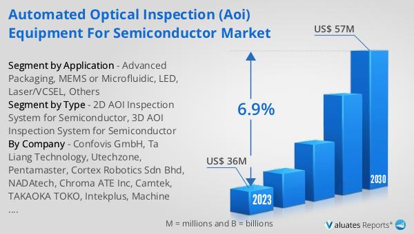
The global Automated Optical Inspection (AOI) Equipment for Semiconductor market was valued at US$ 36 million in 2023 and is anticipated to reach US$ 57 million by 2030, witnessing a CAGR of 6.9% during the forecast period from 2024 to 2030. This growth reflects the increasing demand for high-quality semiconductor devices across various industries, including consumer electronics, automotive, telecommunications, and industrial sectors. The adoption of AOI equipment is driven by the need to ensure the quality and reliability of semiconductor products, as even minor defects can lead to significant performance issues. The market's expansion is also supported by advancements in AOI technology, such as the development of more sophisticated imaging techniques and software algorithms that enhance the accuracy and efficiency of defect detection. As the complexity of semiconductor devices continues to grow, the demand for advanced AOI solutions is expected to rise, further driving the market's growth. The increasing focus on automation and the integration of AI and machine learning in AOI systems are also contributing to the market's positive outlook. These advancements enable more precise and efficient inspections, reducing the risk of defects and improving overall production yields. The global AOI equipment market is poised for significant growth, reflecting the critical role of AOI technology in ensuring the quality and reliability of modern semiconductor devices.
| Report Metric | Details |
| Report Name | Automated Optical Inspection (AOI) Equipment for Semiconductor Market |
| Accounted market size in 2023 | US$ 36 million |
| Forecasted market size in 2030 | US$ 57 million |
| CAGR | 6.9% |
| Base Year | 2023 |
| Forecasted years | 2024 - 2030 |
| Segment by Type |
|
| Segment by Application |
|
| Production by Region |
|
| Consumption by Region |
|
| By Company | Confovis GmbH, Ta Liang Technology, Utechzone, Pentamaster, Cortex Robotics Sdn Bhd, NADAtech, Chroma ATE Inc, Camtek, TAKAOKA TOKO, Intekplus, Machine Vision Products, Inc., SMEE, The First Contact Tech(TFCT), Koh Young Technology, Test Research, ViTrox, Saki Corporation, Cyberoptics Corporation, Omron Corporation, Viscom, Mirtec, Parmi Corp, VI Technology (Mycronic), GÖPEL electronic GmbH, Mek Marantz Electronics, Nordson YESTECH, PEMTRON, Hangzhou Changchuan Technology |
| Forecast units | USD million in value |
| Report coverage | Revenue and volume forecast, company share, competitive landscape, growth factors and trends |


