What is Global Bump AOI System Market?
The Global Bump AOI (Automated Optical Inspection) System Market is a specialized segment within the broader semiconductor and electronics inspection industry. This market focuses on the development and deployment of advanced AOI systems designed to inspect bumps on semiconductor wafers and substrates. These bumps are tiny solder balls or pillars that serve as electrical connections between the semiconductor die and the package or between different layers of a multi-layer package. The primary goal of Bump AOI systems is to ensure the quality and reliability of these connections, which are critical for the performance and longevity of electronic devices. The market encompasses various types of AOI systems, including those for package substrates, wafers, and panel-level packaging. These systems utilize cutting-edge technologies such as high-resolution imaging, machine learning, and advanced algorithms to detect defects, measure bump dimensions, and verify alignment. The increasing complexity of semiconductor devices and the growing demand for miniaturization in electronics are driving the need for more sophisticated Bump AOI systems. As a result, the Global Bump AOI System Market is experiencing significant growth, with manufacturers continuously innovating to meet the evolving needs of the semiconductor industry.
Package Substrate Bump AOI, Wafer / PLP Bump AOI in the Global Bump AOI System Market:
Package Substrate Bump AOI and Wafer/PLP Bump AOI are two critical segments within the Global Bump AOI System Market. Package Substrate Bump AOI systems are designed to inspect bumps on package substrates, which are the base materials used to support and interconnect semiconductor devices. These systems play a crucial role in ensuring the quality and reliability of the bumps, which are essential for the electrical performance of the final packaged device. They utilize high-resolution cameras and advanced image processing algorithms to detect defects such as missing bumps, misalignment, and size variations. On the other hand, Wafer/PLP (Panel Level Packaging) Bump AOI systems are used to inspect bumps on semiconductor wafers and panel-level packages. These systems are essential for the early detection of defects during the wafer fabrication process, which can significantly reduce the cost and time associated with downstream rework and repairs. Wafer/PLP Bump AOI systems employ a combination of optical inspection, 3D measurement, and machine learning techniques to accurately identify and classify defects. They are capable of inspecting a wide range of bump types, including micro-bumps, copper pillars, and solder balls, across various wafer sizes and panel formats. The integration of these AOI systems into the semiconductor manufacturing process helps to improve yield, enhance product quality, and reduce production costs. As the demand for smaller, more powerful electronic devices continues to grow, the importance of Package Substrate Bump AOI and Wafer/PLP Bump AOI systems in ensuring the reliability and performance of semiconductor devices cannot be overstated.
Bump-AOI for FC-BGA and FC-CSP, Bump-AOI for Full-Panel/Q-Panel and WLCSP in the Global Bump AOI System Market:
The usage of Global Bump AOI System Market in areas such as Bump-AOI for FC-BGA (Flip Chip Ball Grid Array) and FC-CSP (Flip Chip Chip Scale Package), Bump-AOI for Full-Panel/Q-Panel, and WLCSP (Wafer Level Chip Scale Package) is extensive and multifaceted. Bump-AOI systems for FC-BGA and FC-CSP are designed to inspect the bumps on flip chip packages, which are widely used in high-performance computing, telecommunications, and consumer electronics. These systems ensure that the bumps are correctly formed, properly aligned, and free from defects, which is critical for the electrical performance and reliability of the final product. They use advanced imaging and analysis techniques to detect issues such as missing bumps, misalignment, and size variations. Bump-AOI systems for Full-Panel/Q-Panel are used to inspect bumps on large panel substrates, which are increasingly being used in advanced packaging technologies such as fan-out wafer-level packaging (FOWLP) and panel-level packaging (PLP). These systems are capable of inspecting a large number of bumps simultaneously, providing high throughput and accuracy. They utilize high-resolution cameras, 3D measurement technologies, and sophisticated algorithms to detect and classify defects. WLCSP Bump-AOI systems are designed to inspect bumps on wafer-level chip scale packages, which are used in a wide range of applications, including mobile devices, automotive electronics, and IoT devices. These systems ensure that the bumps are correctly formed and free from defects, which is essential for the performance and reliability of the final product. They use a combination of optical inspection, 3D measurement, and machine learning techniques to accurately identify and classify defects. The integration of Bump-AOI systems into the manufacturing process helps to improve yield, enhance product quality, and reduce production costs, making them an essential tool for the semiconductor industry.
Global Bump AOI System Market Outlook:
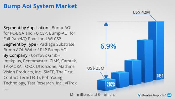
The global Bump AOI System market was valued at US$ 25 million in 2023 and is anticipated to reach US$ 42 million by 2030, witnessing a CAGR of 6.9% during the forecast period 2024-2030. This growth is driven by the increasing demand for high-performance and miniaturized electronic devices, which require advanced packaging technologies and reliable interconnects. Bump AOI systems play a crucial role in ensuring the quality and reliability of these interconnects, which are essential for the performance and longevity of electronic devices. The market is characterized by continuous innovation and technological advancements, with manufacturers developing more sophisticated AOI systems to meet the evolving needs of the semiconductor industry. These systems utilize cutting-edge technologies such as high-resolution imaging, 3D measurement, and machine learning to detect and classify defects, measure bump dimensions, and verify alignment. The integration of these systems into the semiconductor manufacturing process helps to improve yield, enhance product quality, and reduce production costs. As a result, the Global Bump AOI System Market is expected to experience significant growth over the forecast period, driven by the increasing complexity of semiconductor devices and the growing demand for miniaturization in electronics.
| Report Metric | Details |
| Report Name | Bump AOI System Market |
| Accounted market size in 2023 | US$ 25 million |
| Forecasted market size in 2030 | US$ 42 million |
| CAGR | 6.9% |
| Base Year | 2023 |
| Forecasted years | 2024 - 2030 |
| Segment by Type |
|
| Segment by Application |
|
| Production by Region |
|
| Consumption by Region |
|
| By Company | Confovis GmbH, Intekplus, Pentamaster, CIMS, Camtek, TAKAOKA TOKO, Utechzone, Machine Vision Products, Inc., SMEE, The First Contact Tech(TFCT), Koh Young Technology, Test Research, Inc., ViTrox Corporation Berhad, Cyberoptics Corporation, Omron, Mirtec, Parmi Corp, Cortex Robotics Sdn Bhd, Nordson YESTECH, PEMTRON, Hangzhou Changchuan Technology |
| Forecast units | USD million in value |
| Report coverage | Revenue and volume forecast, company share, competitive landscape, growth factors and trends |


