What is Global Glass Wafer Dicing Service Market?
The Global Glass Wafer Dicing Service Market is a specialized segment within the semiconductor industry that focuses on the precise cutting and separation of glass wafers. These wafers are essential components in various electronic devices, including integrated circuits, sensors, and microelectromechanical systems (MEMS). The dicing process involves slicing the glass wafers into smaller, usable pieces without causing damage or contamination. This market is driven by the increasing demand for miniaturized electronic devices and advancements in semiconductor technology. Companies offering glass wafer dicing services utilize advanced techniques and equipment to ensure high precision and efficiency. The market is characterized by continuous innovation and the adoption of new technologies to meet the evolving needs of the semiconductor industry.

Water Jet Cutting, Wire Saw Cutting, Other in the Global Glass Wafer Dicing Service Market:
Water Jet Cutting, Wire Saw Cutting, and other methods are integral to the Global Glass Wafer Dicing Service Market. Water Jet Cutting uses a high-pressure stream of water mixed with abrasive materials to cut through glass wafers. This method is highly precise and minimizes thermal damage, making it suitable for delicate and intricate designs. It is also environmentally friendly as it does not produce harmful by-products. Wire Saw Cutting, on the other hand, involves using a thin wire coated with abrasive particles to slice through the glass wafers. This technique is known for its accuracy and ability to produce smooth edges, which are crucial for the performance of electronic components. Wire Saw Cutting is particularly effective for cutting thick or hard materials that are challenging to process with other methods. Other dicing methods in the market include laser cutting and mechanical sawing. Laser cutting uses focused laser beams to cut through the glass wafers with high precision and speed. It is ideal for applications requiring complex shapes and fine details. Mechanical sawing, although less advanced than other methods, is still widely used due to its cost-effectiveness and simplicity. Each of these dicing methods has its advantages and is chosen based on the specific requirements of the application. The choice of dicing method depends on factors such as the thickness of the wafer, the desired precision, and the type of material being processed. The Global Glass Wafer Dicing Service Market continues to evolve with advancements in technology, leading to the development of more efficient and precise dicing techniques. Companies in this market are constantly innovating to improve the quality and performance of their services, ensuring they meet the stringent demands of the semiconductor industry.
Laboratory, Factory in the Global Glass Wafer Dicing Service Market:
The usage of Global Glass Wafer Dicing Service Market in laboratories and factories is crucial for the development and production of advanced electronic devices. In laboratories, glass wafer dicing services are used for research and development purposes. Scientists and engineers rely on these services to create prototypes and test new designs. The precision and accuracy of the dicing process are essential for ensuring the reliability and performance of the experimental devices. Laboratories often require small quantities of diced wafers with specific dimensions and characteristics, making the flexibility and customization offered by dicing service providers invaluable. In factories, glass wafer dicing services are used for mass production of electronic components. The efficiency and speed of the dicing process are critical for meeting production targets and maintaining cost-effectiveness. Factories require large volumes of diced wafers with consistent quality and minimal defects. The advanced dicing techniques used in the Global Glass Wafer Dicing Service Market ensure that the wafers meet the stringent quality standards required for commercial production. The integration of automated systems and robotics in the dicing process further enhances productivity and reduces the risk of human error. Both laboratories and factories benefit from the continuous advancements in dicing technology, which lead to improved performance, higher yields, and reduced costs. The Global Glass Wafer Dicing Service Market plays a vital role in supporting the innovation and growth of the semiconductor industry by providing the necessary tools and services for the development and production of cutting-edge electronic devices.
Global Glass Wafer Dicing Service Market Outlook:
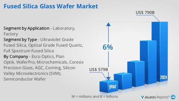
The global market for semiconductors was valued at approximately US$ 579 billion in 2022 and is anticipated to reach around US$ 790 billion by 2029, reflecting a compound annual growth rate (CAGR) of 6% over the forecast period. This growth is driven by the increasing demand for electronic devices, advancements in technology, and the expansion of applications in various industries. The semiconductor market is a critical component of the global economy, influencing the development and production of a wide range of products, from consumer electronics to industrial machinery. The projected growth underscores the importance of continuous innovation and investment in semiconductor technology to meet the evolving needs of the market. Companies operating in this sector are focusing on enhancing their production capabilities, improving product quality, and expanding their market presence to capitalize on the growing demand. The robust growth prospects of the semiconductor market highlight the dynamic nature of the industry and its significant impact on technological progress and economic development.
| Report Metric | Details |
| Report Name | Glass Wafer Dicing Service Market |
| Accounted market size in year | US$ 579 billion |
| Forecasted market size in 2029 | US$ 790 billion |
| CAGR | 6% |
| Base Year | year |
| Forecasted years | 2024 - 2029 |
| Segment by Type |
|
| Segment by Application |
|
| By Region |
|
| By Company | Coresix Precision Glass, Sydor Optics, Specialty Glass Products, Kadco Ceramics, Citrogene, American Precision Dicing, Innovative Fabrication, IRD Glass, Valley Design, Hausser Scientific, NanoSD |
| Forecast units | USD million in value |
| Report coverage | Revenue and volume forecast, company share, competitive landscape, growth factors and trends |