What is Global Plasma Surface Treatment Equipment for Semiconductor Market?
Global Plasma Surface Treatment Equipment for the Semiconductor Market refers to the specialized machinery used to modify the surface properties of semiconductor materials through plasma technology. Plasma, often described as the fourth state of matter, is an ionized gas that can be used to clean, etch, or deposit materials on semiconductor surfaces. This equipment is crucial in the semiconductor manufacturing process as it enhances the adhesion properties, removes contaminants, and prepares surfaces for subsequent processing steps. The demand for plasma surface treatment equipment is driven by the increasing complexity and miniaturization of semiconductor devices, which require precise and efficient surface modification techniques. As the semiconductor industry continues to evolve, the need for advanced plasma treatment solutions becomes more pronounced, making this equipment an integral part of the production process. The global market for this equipment is characterized by technological advancements, increasing investments in semiconductor manufacturing, and a growing emphasis on improving production efficiency and product quality. Companies operating in this market are focused on developing innovative solutions to meet the diverse needs of semiconductor manufacturers, ensuring that they can produce high-performance, reliable, and cost-effective semiconductor devices.
Low Pressure/Vacuum Plasma Surface Treatment Equipment, Atmospheric Plasma Surface Treatment Equipment in the Global Plasma Surface Treatment Equipment for Semiconductor Market:
Low Pressure/Vacuum Plasma Surface Treatment Equipment and Atmospheric Plasma Surface Treatment Equipment are two primary types of plasma treatment technologies used in the semiconductor industry. Low Pressure/Vacuum Plasma Surface Treatment Equipment operates under reduced pressure conditions, typically in a vacuum chamber. This environment allows for precise control over the plasma process, making it ideal for applications that require uniform treatment and minimal contamination. The vacuum conditions enable the use of a wide range of gases, which can be tailored to achieve specific surface modifications. This type of equipment is particularly effective for cleaning, etching, and activating surfaces, as well as for depositing thin films. The controlled environment ensures that the treatment is consistent and repeatable, which is crucial for maintaining the quality and performance of semiconductor devices. On the other hand, Atmospheric Plasma Surface Treatment Equipment operates at atmospheric pressure, eliminating the need for a vacuum chamber. This makes the equipment more versatile and easier to integrate into existing production lines. Atmospheric plasma is generated using a high-voltage electrical discharge, which creates a reactive plasma that can be used for surface cleaning, activation, and coating. This type of equipment is often used for treating larger surfaces or materials that are sensitive to vacuum conditions. The ability to operate at atmospheric pressure also allows for continuous processing, which can enhance production efficiency. Both types of plasma treatment equipment play a vital role in the semiconductor manufacturing process, offering unique advantages and capabilities that cater to different application requirements. As the demand for advanced semiconductor devices continues to grow, the need for efficient and effective plasma surface treatment solutions becomes increasingly important. Manufacturers are continually exploring new technologies and processes to improve the performance and reliability of their products, making plasma treatment equipment an essential component of the semiconductor production landscape.
Chip Bonding, Lead Frame, Others in the Global Plasma Surface Treatment Equipment for Semiconductor Market:
The usage of Global Plasma Surface Treatment Equipment in the semiconductor market spans several critical areas, including chip bonding, lead frame processing, and other applications. In chip bonding, plasma treatment is used to enhance the adhesion properties of semiconductor surfaces, ensuring that chips are securely attached to substrates or other components. This is particularly important in the production of advanced semiconductor devices, where reliable bonding is essential for maintaining electrical connectivity and mechanical stability. Plasma treatment can effectively remove organic contaminants and oxides from surfaces, creating a clean and activated surface that promotes strong adhesion. In lead frame processing, plasma treatment is used to prepare the metal surfaces for subsequent plating or bonding processes. The treatment removes oxides and other contaminants, ensuring that the lead frames have a clean and uniform surface that is conducive to high-quality plating. This is crucial for ensuring the reliability and performance of semiconductor packages, as any defects in the lead frame can lead to electrical failures or reduced device performance. Plasma treatment also plays a role in other semiconductor applications, such as wafer cleaning, surface activation, and thin film deposition. In wafer cleaning, plasma treatment is used to remove residues and contaminants from the wafer surface, ensuring that it is free from particles that could affect device performance. Surface activation is another critical application, where plasma treatment is used to modify the surface energy of materials, enhancing their wettability and adhesion properties. This is particularly important in processes such as photoresist coating, where uniform adhesion is essential for achieving high-resolution patterns. Thin film deposition is another area where plasma treatment is used to deposit uniform and high-quality films on semiconductor surfaces. This is essential for creating the various layers and structures that make up semiconductor devices. Overall, plasma surface treatment equipment plays a vital role in ensuring the quality, reliability, and performance of semiconductor devices, making it an indispensable tool in the semiconductor manufacturing process.
Global Plasma Surface Treatment Equipment for Semiconductor Market Outlook:
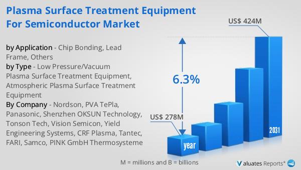
The global market for Plasma Surface Treatment Equipment for Semiconductors was valued at approximately $278 million in 2024. It is anticipated to expand to a revised size of around $424 million by 2031, reflecting a compound annual growth rate (CAGR) of 6.3% over the forecast period. This growth trajectory underscores the increasing demand for advanced plasma treatment solutions in the semiconductor industry. As semiconductor devices become more complex and miniaturized, the need for precise and efficient surface modification techniques becomes more critical. Plasma surface treatment equipment offers the necessary capabilities to meet these demands, providing manufacturers with the tools they need to produce high-performance and reliable semiconductor devices. The market's growth is also driven by technological advancements, increasing investments in semiconductor manufacturing, and a growing emphasis on improving production efficiency and product quality. Companies operating in this market are focused on developing innovative solutions to meet the diverse needs of semiconductor manufacturers, ensuring that they can produce high-performance, reliable, and cost-effective semiconductor devices. As the semiconductor industry continues to evolve, the demand for plasma surface treatment equipment is expected to grow, making it an integral part of the production process.
| Report Metric | Details |
| Report Name | Plasma Surface Treatment Equipment for Semiconductor Market |
| Accounted market size in year | US$ 278 million |
| Forecasted market size in 2031 | US$ 424 million |
| CAGR | 6.3% |
| Base Year | year |
| Forecasted years | 2025 - 2031 |
| by Type |
|
| by Application |
|
| Production by Region |
|
| Consumption by Region |
|
| By Company | Nordson, PVA TePla, Panasonic, Shenzhen OKSUN Technology, Tonson Tech, Vision Semicon, Yield Engineering Systems, CRF Plasma, Tantec, FARI, Samco, PINK GmbH Thermosysteme |
| Forecast units | USD million in value |
| Report coverage | Revenue and volume forecast, company share, competitive landscape, growth factors and trends |


