What is Global Plasma Spray Coating for Semiconductor Market?
Global Plasma Spray Coating for Semiconductor Market is a specialized segment within the broader semiconductor industry that focuses on the application of plasma spray coatings to semiconductor components. This market is driven by the need for advanced protective coatings that enhance the performance and longevity of semiconductor parts. Plasma spray coating is a process that involves the use of a plasma jet to melt and propel coating materials onto a substrate, creating a protective layer. This technique is particularly valuable in the semiconductor industry due to its ability to produce coatings that can withstand high temperatures, corrosive environments, and mechanical wear. The coatings are typically applied to semiconductor etching parts and deposition equipment parts, which are critical components in the manufacturing of semiconductors. The demand for plasma spray coatings in this market is fueled by the continuous advancements in semiconductor technology, which require components that can operate reliably under increasingly demanding conditions. As the semiconductor industry continues to grow, the Global Plasma Spray Coating for Semiconductor Market is expected to expand, driven by the need for high-performance coatings that can meet the stringent requirements of modern semiconductor manufacturing processes.
Atmospheric Plasma Spraying (APS), Vacuum Plasma Spraying (VPS) in the Global Plasma Spray Coating for Semiconductor Market:
Atmospheric Plasma Spraying (APS) and Vacuum Plasma Spraying (VPS) are two prominent techniques used in the Global Plasma Spray Coating for Semiconductor Market. APS is a process that involves the use of a plasma jet to heat and accelerate powdered coating materials, which are then deposited onto a substrate. This technique is performed in an open atmosphere, making it a versatile and cost-effective option for applying coatings to semiconductor components. APS is particularly suitable for applications where the coating needs to be applied quickly and efficiently, and where the substrate can tolerate exposure to the atmosphere during the coating process. The coatings produced by APS are known for their excellent adhesion, thermal resistance, and ability to protect against corrosion and wear. On the other hand, Vacuum Plasma Spraying (VPS) is a more controlled process that takes place in a vacuum chamber. This environment allows for the deposition of coatings with minimal oxidation and contamination, resulting in high-purity coatings that are ideal for semiconductor applications. VPS is often used for coating components that require extremely high levels of cleanliness and precision, such as those used in semiconductor etching and deposition equipment. The vacuum environment also enables the use of reactive gases, which can enhance the properties of the coating. Both APS and VPS play crucial roles in the semiconductor industry by providing coatings that enhance the durability and performance of critical components. The choice between APS and VPS depends on the specific requirements of the application, including factors such as the desired coating properties, the nature of the substrate, and the operating conditions of the component. As the demand for advanced semiconductor devices continues to rise, the use of APS and VPS in the Global Plasma Spray Coating for Semiconductor Market is expected to grow, driven by the need for coatings that can meet the increasingly stringent demands of modern semiconductor manufacturing.
Semiconductor Etching Parts, Semiconductor Deposition Equipment Parts in the Global Plasma Spray Coating for Semiconductor Market:
The Global Plasma Spray Coating for Semiconductor Market finds significant application in the areas of semiconductor etching parts and semiconductor deposition equipment parts. Semiconductor etching parts are critical components used in the etching process, which involves the removal of material from the surface of a semiconductor wafer to create intricate patterns and structures. Plasma spray coatings are applied to these parts to enhance their resistance to the harsh chemical and physical conditions encountered during the etching process. The coatings provide a protective barrier that prevents corrosion and wear, ensuring the longevity and reliability of the etching parts. This is particularly important in the semiconductor industry, where precision and consistency are paramount. Similarly, semiconductor deposition equipment parts benefit from plasma spray coatings due to the demanding conditions they face during the deposition process. Deposition equipment is used to apply thin films of material onto semiconductor wafers, a process that requires high levels of precision and control. Plasma spray coatings help to protect the deposition equipment parts from the high temperatures and corrosive environments encountered during this process, ensuring their durability and performance. The coatings also contribute to the overall efficiency and effectiveness of the deposition process by minimizing downtime and maintenance requirements. As the semiconductor industry continues to advance, the demand for high-performance coatings for etching and deposition equipment parts is expected to increase, driving growth in the Global Plasma Spray Coating for Semiconductor Market. The ability of plasma spray coatings to enhance the performance and longevity of critical semiconductor components makes them an essential part of modern semiconductor manufacturing.
Global Plasma Spray Coating for Semiconductor Market Outlook:
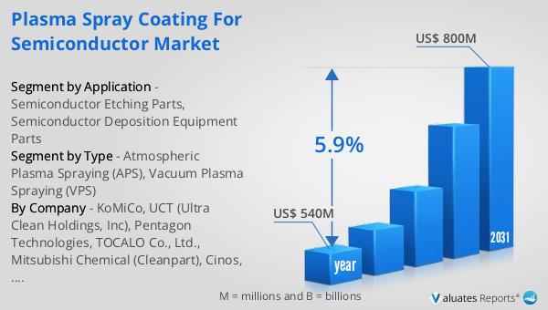
In 2024, the global market for Plasma Spray Coating for Semiconductor was valued at approximately $540 million. This market is anticipated to grow significantly, reaching an estimated value of $800 million by 2031. This growth represents a compound annual growth rate (CAGR) of 5.9% over the forecast period. The increasing demand for advanced semiconductor devices, coupled with the need for high-performance coatings that can withstand the rigorous conditions of semiconductor manufacturing, is driving this growth. Plasma spray coatings are essential for enhancing the durability and performance of semiconductor components, making them a critical part of the semiconductor manufacturing process. As the semiconductor industry continues to evolve, the demand for plasma spray coatings is expected to rise, contributing to the overall growth of the market. The projected growth of the Global Plasma Spray Coating for Semiconductor Market reflects the increasing importance of these coatings in the semiconductor industry and their role in enabling the production of advanced semiconductor devices. The market's expansion is also indicative of the broader trends in the semiconductor industry, including the push for smaller, more powerful, and more efficient devices. As a result, the Global Plasma Spray Coating for Semiconductor Market is poised for continued growth and development in the coming years.
| Report Metric | Details |
| Report Name | Plasma Spray Coating for Semiconductor Market |
| Accounted market size in year | US$ 540 million |
| Forecasted market size in 2031 | US$ 800 million |
| CAGR | 5.9% |
| Base Year | year |
| Forecasted years | 2025 - 2031 |
| Segment by Type |
|
| Segment by Application |
|
| By Region |
|
| By Company | KoMiCo, UCT (Ultra Clean Holdings, Inc), Pentagon Technologies, TOCALO Co., Ltd., Mitsubishi Chemical (Cleanpart), Cinos, Hansol IONES, WONIK QnC, DFtech, TOPWINTECH, Oerlikon Balzers, Frontken Corporation Berhad, Hung Jie Technology Corporation, Jiangsu Kaiweitesi Semiconductor Technology Co., Ltd., HCUT Co., Ltd, Shanghai Companion, Value Engineering Co., Ltd, Chongqing Genori Technology Co., Ltd, Aldon Group, Vivid Inc. |
| Forecast units | USD million in value |
| Report coverage | Revenue and volume forecast, company share, competitive landscape, growth factors and trends |


