What is Global SiC Wafer Processing Equipment Market?
The Global SiC Wafer Processing Equipment Market is a specialized segment within the semiconductor industry, focusing on the tools and machinery used to process silicon carbide (SiC) wafers. SiC is a compound semiconductor material known for its superior thermal conductivity, high electric field strength, and wide bandgap, making it ideal for high-power and high-temperature applications. The market for SiC wafer processing equipment is driven by the increasing demand for SiC-based devices in various industries, including automotive, telecommunications, and energy. These devices are essential for electric vehicles, 5G technology, and renewable energy systems, where efficiency and performance are critical. The equipment used in this market includes tools for wafer slicing, polishing, cleaning, and etching, among others. As the demand for SiC devices grows, so does the need for advanced processing equipment that can handle the unique properties of SiC materials. This market is characterized by rapid technological advancements and a focus on precision and efficiency to meet the stringent requirements of SiC wafer processing. Companies in this market are continually innovating to improve the quality and yield of SiC wafers, which are crucial for the performance of the final semiconductor devices.
SiC Thinning and CMP, SiC Deposition Equipment, SiC Epitaxy/HTCVD Equipment, SiC Thermal Processing Equipment, SiC Etch and Clean Equipment, SiC Ion Implant, SiC Patterning Equipment, SiC Metrology and Inspection Equipment, SiC Wafer Bonders in the Global SiC Wafer Processing Equipment Market:
Silicon carbide (SiC) wafer processing involves several critical steps, each requiring specialized equipment to ensure the highest quality and performance of the final semiconductor devices. SiC Thinning and Chemical Mechanical Planarization (CMP) are essential processes that reduce the wafer's thickness and smooth its surface, respectively. Thinning is crucial for achieving the desired electrical characteristics, while CMP ensures a defect-free surface, which is vital for subsequent processing steps. SiC Deposition Equipment is used to deposit thin films of materials onto the wafer surface, a process necessary for creating various device structures. This equipment must be capable of handling the high temperatures and corrosive environments associated with SiC processing. SiC Epitaxy/HTCVD Equipment is used to grow high-quality SiC layers on substrates, a critical step for producing SiC-based power devices. High-Temperature Chemical Vapor Deposition (HTCVD) is a common method for epitaxial growth, requiring precise control over temperature and gas flow to achieve the desired layer properties. SiC Thermal Processing Equipment is used for annealing and other heat treatments, which are essential for activating dopants and repairing crystal defects. These processes require equipment that can maintain uniform temperature distribution across the wafer. SiC Etch and Clean Equipment are used to pattern and clean the wafer surface, removing unwanted material and contaminants. Etching is a critical step in defining device features, while cleaning ensures that the wafer surface is free of particles and residues that could affect device performance. SiC Ion Implant Equipment is used to introduce dopants into the SiC wafer, a process that modifies the electrical properties of the material. This equipment must be capable of delivering precise doses of ions with high accuracy. SiC Patterning Equipment is used to create the intricate patterns required for semiconductor devices. This involves photolithography and other techniques that require high precision and alignment accuracy. SiC Metrology and Inspection Equipment are used to measure and inspect the wafer at various stages of processing, ensuring that it meets the required specifications. This equipment is essential for quality control and yield improvement. Finally, SiC Wafer Bonders are used to bond SiC wafers to other materials, a process that is often required for creating complex device structures. This equipment must be capable of handling the high temperatures and pressures involved in the bonding process. Each of these equipment types plays a crucial role in the SiC wafer processing market, contributing to the production of high-performance SiC devices.
SiC Substrate Processing, SiC Epitaxy Processing, SiC Devices Fabrication in the Global SiC Wafer Processing Equipment Market:
The Global SiC Wafer Processing Equipment Market plays a vital role in various stages of SiC semiconductor device manufacturing, including SiC Substrate Processing, SiC Epitaxy Processing, and SiC Devices Fabrication. In SiC Substrate Processing, the focus is on preparing the raw SiC material into a usable wafer form. This involves slicing the bulk SiC crystal into thin wafers, followed by polishing and cleaning to achieve a smooth, defect-free surface. The equipment used in this stage must be capable of handling the hardness and brittleness of SiC, ensuring minimal damage and high yield. SiC Epitaxy Processing involves the growth of high-quality SiC layers on the substrate, a critical step for creating the active regions of semiconductor devices. This process requires precise control over temperature, gas flow, and deposition rates to achieve the desired layer thickness and uniformity. The equipment used in epitaxy processing must be able to operate at high temperatures and in corrosive environments, as SiC epitaxial growth often involves harsh chemical reactions. In SiC Devices Fabrication, the processed wafers undergo various steps to create the final semiconductor devices. This includes patterning, doping, etching, and metallization, each requiring specialized equipment to achieve the desired device characteristics. The equipment used in this stage must be capable of handling the unique properties of SiC, such as its high thermal conductivity and wide bandgap, to ensure optimal device performance. Throughout these stages, the Global SiC Wafer Processing Equipment Market provides the necessary tools and technologies to produce high-quality SiC devices, which are essential for applications in power electronics, telecommunications, and renewable energy. The demand for SiC devices is driven by their superior performance in high-power and high-temperature environments, making them ideal for electric vehicles, 5G infrastructure, and solar inverters. As the market for SiC devices continues to grow, so does the need for advanced processing equipment that can meet the stringent requirements of SiC wafer processing.
Global SiC Wafer Processing Equipment Market Outlook:
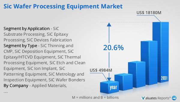
The outlook for the Global SiC Wafer Processing Equipment Market is promising, with significant growth expected over the coming years. In 2024, the market was valued at approximately US$ 4,984 million. By 2031, it is anticipated to expand to a revised size of US$ 18,180 million, reflecting a robust compound annual growth rate (CAGR) of 20.6% during the forecast period. This growth is driven by the increasing demand for SiC-based devices across various industries, including automotive, telecommunications, and energy. The superior properties of SiC, such as its high thermal conductivity and electric field strength, make it an ideal material for high-power and high-temperature applications. As a result, there is a growing need for advanced processing equipment that can handle the unique challenges of SiC wafer manufacturing. Companies in this market are investing in research and development to innovate and improve the efficiency and precision of their equipment, ensuring they can meet the evolving needs of the semiconductor industry. The expansion of the SiC Wafer Processing Equipment Market is also supported by the increasing adoption of electric vehicles, 5G technology, and renewable energy systems, all of which rely on SiC devices for enhanced performance and efficiency. As these industries continue to grow, the demand for SiC wafer processing equipment is expected to rise, driving further market expansion.
| Report Metric | Details |
| Report Name | SiC Wafer Processing Equipment Market |
| Accounted market size in year | US$ 4984 million |
| Forecasted market size in 2031 | US$ 18180 million |
| CAGR | 20.6% |
| Base Year | year |
| Forecasted years | 2025 - 2031 |
| Segment by Type |
|
| Segment by Application |
|
| By Region |
|
| By Company | Applied Materials, ACCRETECH, Engis, Revasum, DISCO, Wolfspeed, SiCrystal, II-VI Advanced Materials, TankeBlue, PVA Tepla, Materials Research Furnaces, Aymont, Takatori, Meyer Burger, Komatsu NTC, KLA Corporation, Lasertec, Aixtron, LPE Epitaxial Technology, VEECO, AMEC, NuFlare Technology Inc., Taiyo Nippon Sanso, ASM International N.V, Naura, Logitech, 3D-Micromac, Synova S.A., Visiontec Group, Nanotronics, TASMIT, Inc. (Toray Engineering), Angkun Vision (Beijing) Technology, Beijing TSD Semiconductor Co., Ltd., Zhejiang Jingsheng Mechanical & Electrical, Shanxi Semisic Crystal Co., Ltd., Shenzhen Naso Tech Co., Ltd., TDG Holding, Xin San Dai Semiconductor Technology, PNC Technology Group, Hebei arashi whale photoelectric technology, Nanjing Jingsheng Equipment, Beijing Jingyuntong Technology |
| Forecast units | USD million in value |
| Report coverage | Revenue and volume forecast, company share, competitive landscape, growth factors and trends |


