What is Global SiC Metrology and Inspection Equipment Market?
The Global SiC Metrology and Inspection Equipment Market is a specialized segment within the semiconductor industry that focuses on the tools and technologies used to measure and inspect silicon carbide (SiC) materials. SiC is a compound semiconductor that offers superior performance in high-temperature and high-voltage applications compared to traditional silicon. This makes it highly desirable for use in power electronics, electric vehicles, and renewable energy systems. The metrology and inspection equipment in this market are crucial for ensuring the quality and reliability of SiC wafers and devices. These tools help in identifying defects, measuring dimensions, and ensuring that the SiC materials meet the stringent specifications required for their intended applications. As the demand for SiC-based technologies grows, the market for these specialized equipment is also expanding, driven by the need for precision and efficiency in the manufacturing process. The market is characterized by rapid technological advancements and a high level of competition among key players who are continuously innovating to meet the evolving needs of the semiconductor industry.
SiC Defect Inspection Equipment, SiC Metrology Equipment in the Global SiC Metrology and Inspection Equipment Market:
SiC Defect Inspection Equipment and SiC Metrology Equipment are integral components of the Global SiC Metrology and Inspection Equipment Market. SiC Defect Inspection Equipment is designed to detect and analyze defects in silicon carbide wafers. These defects can include dislocations, micropipes, and other imperfections that can affect the performance and reliability of SiC-based devices. The equipment uses advanced imaging and scanning technologies to provide detailed information about the location, size, and nature of these defects. This information is crucial for manufacturers to improve their production processes and ensure the quality of their products. On the other hand, SiC Metrology Equipment is used to measure the physical and electrical properties of SiC wafers. This includes measuring parameters such as thickness, flatness, and resistivity. The equipment employs a variety of techniques, including optical and electrical measurements, to provide accurate and reliable data. This data is essential for ensuring that the wafers meet the required specifications and for optimizing the manufacturing process. Both types of equipment are critical for the production of high-quality SiC wafers and devices, and they play a vital role in the growth and development of the SiC industry. As the demand for SiC-based technologies continues to rise, the need for advanced metrology and inspection equipment is also increasing, driving innovation and competition in the market.
SiC Substrate/Wafer, SiC Epitaxial Wafer in the Global SiC Metrology and Inspection Equipment Market:
The usage of Global SiC Metrology and Inspection Equipment Market in areas such as SiC Substrate/Wafer and SiC Epitaxial Wafer is crucial for ensuring the quality and performance of these materials. SiC Substrate/Wafer refers to the base material on which SiC devices are built. The quality of the substrate is critical as it directly impacts the performance and reliability of the final device. Metrology and inspection equipment are used to measure and inspect the physical and electrical properties of the substrate, ensuring that it meets the required specifications. This includes measuring parameters such as thickness, flatness, and resistivity, as well as detecting any defects or imperfections. SiC Epitaxial Wafer, on the other hand, refers to a layer of SiC that is grown on top of the substrate. This layer is critical for the performance of the device, as it determines the electrical characteristics of the final product. Metrology and inspection equipment are used to measure the thickness, uniformity, and electrical properties of the epitaxial layer, ensuring that it meets the required specifications. This includes detecting any defects or imperfections that could affect the performance of the device. The use of advanced metrology and inspection equipment is essential for ensuring the quality and reliability of SiC substrates and epitaxial wafers, and it plays a vital role in the growth and development of the SiC industry. As the demand for SiC-based technologies continues to rise, the need for advanced metrology and inspection equipment is also increasing, driving innovation and competition in the market.
Global SiC Metrology and Inspection Equipment Market Outlook:
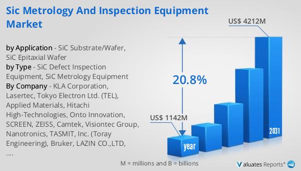
The global market for SiC Metrology and Inspection Equipment was valued at approximately $1,142 million in 2024, with projections indicating a significant growth trajectory, reaching an estimated $4,212 million by 2031. This growth is expected to occur at a compound annual growth rate (CAGR) of 20.8% over the forecast period. The market is highly concentrated, with the top five players commanding around 95% of the total market share. Geographically, North America leads the market, accounting for about 32% of the global share. This is followed by Europe and Japan, which hold shares of approximately 27% and 15%, respectively. The dominance of these regions can be attributed to their advanced technological infrastructure and the presence of key industry players. The rapid growth of the market is driven by the increasing demand for SiC-based technologies in various applications, including power electronics, electric vehicles, and renewable energy systems. As the market continues to expand, companies are investing heavily in research and development to innovate and improve their metrology and inspection equipment, ensuring they meet the evolving needs of the semiconductor industry. This competitive landscape is characterized by rapid technological advancements and a focus on precision and efficiency in the manufacturing process.
| Report Metric | Details |
| Report Name | SiC Metrology and Inspection Equipment Market |
| Accounted market size in year | US$ 1142 million |
| Forecasted market size in 2031 | US$ 4212 million |
| CAGR | 20.8% |
| Base Year | year |
| Forecasted years | 2025 - 2031 |
| by Type |
|
| by Application |
|
| Production by Region |
|
| Consumption by Region |
|
| By Company | KLA Corporation, Lasertec, Tokyo Electron Ltd. (TEL), Applied Materials, Hitachi High-Technologies, Onto Innovation, SCREEN, ZEISS, Camtek, Visiontec Group, Nanotronics, TASMIT, Inc. (Toray Engineering), Bruker, LAZIN CO.,LTD, EtaMax, Angkun Vision (Beijing) Technology, Spirox Corporation, Shenzhen Glint Vision, confovis GmbH, CASI Vision Technology (Luoyang) Co., Ltd, CETC Fenghua Information Equipment, T-Vision.AI (Hangzhou) Tech Co.,Ltd. |
| Forecast units | USD million in value |
| Report coverage | Revenue and volume forecast, company share, competitive landscape, growth factors and trends |


