What is Global Metrology and Inspection Equipment for SiC & GaN Market?
Global Metrology and Inspection Equipment for SiC & GaN Market refers to the specialized tools and technologies used to measure and inspect silicon carbide (SiC) and gallium nitride (GaN) materials. These materials are crucial in the semiconductor industry due to their superior properties, such as high thermal conductivity, high breakdown voltage, and high electron mobility, which make them ideal for high-power and high-frequency applications. Metrology equipment ensures that these materials meet the stringent quality and performance standards required for their use in various applications, including power electronics, radio frequency (RF) devices, and optoelectronics. Inspection equipment, on the other hand, is used to detect and analyze defects in SiC and GaN materials, ensuring that only high-quality materials are used in the manufacturing process. This market is driven by the increasing demand for SiC and GaN materials in various industries, including automotive, telecommunications, and consumer electronics, as these materials enable the development of more efficient and compact electronic devices. As the demand for these materials continues to grow, the need for advanced metrology and inspection equipment is also expected to increase, driving the growth of the global market.
SiC & GaN Defect Inspection Equipment, SiC & GaN Metrology Equipment in the Global Metrology and Inspection Equipment for SiC & GaN Market:
SiC & GaN Defect Inspection Equipment and SiC & GaN Metrology Equipment are integral components of the Global Metrology and Inspection Equipment for SiC & GaN Market. Defect inspection equipment is designed to identify and analyze imperfections in SiC and GaN materials, which can significantly impact the performance and reliability of the final products. These defects can occur during the manufacturing process and may include dislocations, micropipes, and stacking faults. Advanced inspection technologies, such as optical inspection, X-ray diffraction, and scanning electron microscopy, are employed to detect these defects with high precision. The ability to identify and rectify defects early in the production process is crucial for maintaining the quality and performance of SiC and GaN-based devices. On the other hand, SiC & GaN Metrology Equipment focuses on measuring the physical and electrical properties of these materials. This includes assessing parameters such as thickness, roughness, and electrical conductivity, which are critical for ensuring that the materials meet the required specifications for their intended applications. Metrology equipment utilizes a range of techniques, including atomic force microscopy, ellipsometry, and profilometry, to provide accurate and reliable measurements. The integration of advanced metrology and inspection equipment into the manufacturing process helps manufacturers achieve higher yields, reduce production costs, and improve the overall quality of SiC and GaN-based products. As the demand for these materials continues to rise, driven by their applications in electric vehicles, renewable energy systems, and advanced communication technologies, the importance of defect inspection and metrology equipment in ensuring the quality and performance of SiC and GaN materials cannot be overstated. The market for these equipment is expected to grow significantly as manufacturers seek to enhance their production capabilities and meet the increasing demand for high-quality SiC and GaN materials.
SiC Wafer/Epitaxial/Device, GaN Wafer/Epitaxial/Device in the Global Metrology and Inspection Equipment for SiC & GaN Market:
The usage of Global Metrology and Inspection Equipment for SiC & GaN Market is pivotal in the production of SiC and GaN wafers, epitaxial layers, and devices. In the case of SiC wafers, metrology equipment is used to measure the thickness, flatness, and surface roughness of the wafers, ensuring that they meet the stringent specifications required for high-performance applications. Inspection equipment is employed to detect defects such as micropipes and dislocations, which can affect the electrical properties of the wafers. For SiC epitaxial layers, metrology equipment is used to assess the thickness and uniformity of the layers, while inspection equipment is used to identify defects such as stacking faults and basal plane dislocations. These defects can impact the performance and reliability of SiC-based devices, making their detection and analysis crucial for ensuring the quality of the final products. In the case of SiC devices, metrology equipment is used to measure the electrical properties of the devices, such as breakdown voltage and on-resistance, while inspection equipment is used to detect defects that may have occurred during the device fabrication process. Similarly, for GaN wafers, metrology equipment is used to measure the thickness and surface roughness of the wafers, while inspection equipment is used to detect defects such as threading dislocations and pits. For GaN epitaxial layers, metrology equipment is used to assess the thickness and uniformity of the layers, while inspection equipment is used to identify defects such as V-pits and hillocks. These defects can affect the performance of GaN-based devices, making their detection and analysis crucial for ensuring the quality of the final products. In the case of GaN devices, metrology equipment is used to measure the electrical properties of the devices, such as threshold voltage and transconductance, while inspection equipment is used to detect defects that may have occurred during the device fabrication process. The integration of advanced metrology and inspection equipment into the production process helps manufacturers achieve higher yields, reduce production costs, and improve the overall quality of SiC and GaN-based products. As the demand for these materials continues to rise, driven by their applications in power electronics, RF devices, and optoelectronics, the importance of metrology and inspection equipment in ensuring the quality and performance of SiC and GaN materials cannot be overstated.
Global Metrology and Inspection Equipment for SiC & GaN Market Outlook:
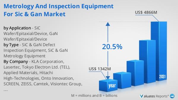
In 2024, the global market for Metrology and Inspection Equipment for SiC and GaN was valued at approximately $1,342 million. It is anticipated to expand significantly, reaching an estimated size of $4,866 million by 2031, with a compound annual growth rate (CAGR) of 20.5% over the forecast period. The market is highly concentrated, with the top five players commanding around 95% of the market share. North America emerges as the largest market, accounting for about 32% of the total market share. Following closely are Europe and Japan, with market shares of 27% and 15%, respectively. This growth trajectory underscores the increasing demand for SiC and GaN materials across various industries, driven by their superior properties and the need for advanced metrology and inspection equipment to ensure the quality and performance of these materials. The significant market share held by North America can be attributed to the region's strong presence in the semiconductor industry and the growing adoption of SiC and GaN materials in applications such as electric vehicles, renewable energy systems, and advanced communication technologies. Europe and Japan also play a crucial role in the market, with their well-established semiconductor industries and increasing focus on developing high-performance electronic devices. As the market continues to evolve, the demand for advanced metrology and inspection equipment is expected to rise, driven by the need to enhance production capabilities and meet the growing demand for high-quality SiC and GaN materials.
| Report Metric | Details |
| Report Name | Metrology and Inspection Equipment for SiC & GaN Market |
| Accounted market size in year | US$ 1342 million |
| Forecasted market size in 2031 | US$ 4866 million |
| CAGR | 20.5% |
| Base Year | year |
| Forecasted years | 2025 - 2031 |
| by Type |
|
| by Application |
|
| Production by Region |
|
| Consumption by Region |
|
| By Company | KLA Corporation, Lasertec, Tokyo Electron Ltd. (TEL), Applied Materials, Hitachi High-Technologies, Onto Innovation, SCREEN, ZEISS, Camtek, Visiontec Group, Nanotronics, TASMIT, Inc. (Toray Engineering), Bruker, LAZIN CO.,LTD, EtaMax, Angkun Vision (Beijing) Technology, Spirox Corporation, Shenzhen Glint Vision, confovis GmbH, CASI Vision Technology (Luoyang) Co., Ltd, CETC Fenghua Information Equipment, T-Vision.AI (Hangzhou) Tech Co.,Ltd. |
| Forecast units | USD million in value |
| Report coverage | Revenue and volume forecast, company share, competitive landscape, growth factors and trends |


