What is Global UBM Plating Service Market?
The Global UBM (Under Bump Metallization) Plating Service Market is a specialized segment within the semiconductor industry that focuses on providing plating services for semiconductor devices. UBM plating is a critical process in the manufacturing of semiconductor components, particularly in the creation of flip-chip packages. This process involves depositing a thin layer of metal onto the semiconductor wafer, which serves as a foundation for solder bumps that connect the chip to the substrate. The UBM layer ensures strong adhesion and electrical conductivity, which are essential for the reliable performance of semiconductor devices. The market for UBM plating services is driven by the increasing demand for advanced semiconductor devices used in various applications, including consumer electronics, automotive, telecommunications, and industrial sectors. As technology continues to evolve, the need for more efficient and reliable semiconductor packaging solutions grows, further propelling the demand for UBM plating services. Companies operating in this market are continually innovating to improve the quality and efficiency of their plating processes, ensuring they meet the stringent requirements of modern semiconductor manufacturing. The global UBM plating service market is characterized by a competitive landscape, with numerous players offering a range of services to meet the diverse needs of their customers.
in the Global UBM Plating Service Market:
The Global UBM Plating Service Market caters to a wide array of customers, each with unique requirements and preferences. Various types of UBM plating services are employed to meet these diverse needs. One of the most common types is electroless nickel plating, which involves the chemical deposition of nickel onto the semiconductor wafer without the use of an electric current. This method is favored for its ability to produce uniform coatings with excellent corrosion resistance and wear properties. Another popular type is electrolytic plating, which uses an electric current to deposit metal onto the wafer. This method allows for precise control over the thickness and composition of the metal layer, making it ideal for applications requiring high precision and reliability. Additionally, some customers opt for gold plating, which provides excellent conductivity and resistance to oxidation, making it suitable for high-performance applications. Silver plating is another option, offering good conductivity and cost-effectiveness for certain applications. Each type of plating service has its advantages and limitations, and the choice often depends on the specific requirements of the semiconductor device being manufactured. For instance, customers in the consumer electronics sector may prioritize cost-effectiveness and high-volume production, leading them to choose electroless nickel or silver plating. In contrast, customers in the automotive or aerospace industries may require the superior performance and reliability offered by gold or electrolytic plating. The choice of plating type is also influenced by factors such as the size and complexity of the semiconductor device, the operating environment, and the desired lifespan of the product. As a result, UBM plating service providers must offer a diverse range of options to cater to the varied needs of their customers. They must also stay abreast of the latest technological advancements and industry trends to ensure they can deliver the most effective and efficient solutions. This requires ongoing investment in research and development, as well as close collaboration with customers to understand their evolving needs and challenges. By offering a comprehensive suite of plating services, providers can position themselves as trusted partners in the semiconductor manufacturing process, helping their customers achieve their performance and cost objectives. The competitive nature of the Global UBM Plating Service Market means that providers must continually innovate and differentiate themselves to maintain a competitive edge. This may involve developing new plating techniques, improving process efficiency, or enhancing the quality and reliability of their services. Ultimately, the success of a UBM plating service provider depends on its ability to deliver high-quality, cost-effective solutions that meet the diverse needs of its customers.
Logic, Memory, Power Semiconductors, MEMS, Others in the Global UBM Plating Service Market:
The Global UBM Plating Service Market plays a crucial role in the production of various semiconductor devices, including logic, memory, power semiconductors, MEMS (Micro-Electro-Mechanical Systems), and others. In the realm of logic semiconductors, UBM plating is essential for creating reliable connections between the chip and the substrate. Logic devices, such as microprocessors and digital signal processors, require precise and robust interconnections to function effectively. UBM plating ensures that these connections are strong and conductive, enabling the efficient transmission of electrical signals. In memory semiconductors, UBM plating is used to enhance the performance and reliability of devices such as DRAM (Dynamic Random Access Memory) and NAND flash memory. These devices are critical components in a wide range of electronic products, from smartphones to data centers. The UBM layer provides a stable foundation for solder bumps, ensuring that the memory chips can withstand the rigors of high-speed data processing and storage. Power semiconductors, which are used to control and convert electrical power in various applications, also benefit from UBM plating. These devices often operate under high current and voltage conditions, making reliable interconnections essential for their performance and longevity. UBM plating provides the necessary adhesion and conductivity to ensure that power semiconductors can handle the demands of modern electronic systems. In the field of MEMS, UBM plating is used to create reliable connections for devices such as sensors and actuators. MEMS devices are often used in applications where size and weight are critical factors, such as in automotive and aerospace systems. The UBM layer ensures that these devices can maintain their performance and reliability even in challenging environments. Beyond these specific applications, UBM plating is also used in a variety of other semiconductor devices, including RF (Radio Frequency) components and optoelectronic devices. In each case, the UBM layer plays a vital role in ensuring the performance, reliability, and longevity of the device. As the demand for advanced semiconductor devices continues to grow, the importance of UBM plating in the manufacturing process becomes increasingly apparent. By providing a reliable and efficient means of creating interconnections, UBM plating enables the development of cutting-edge electronic products that meet the needs of today's consumers and industries.
Global UBM Plating Service Market Outlook:
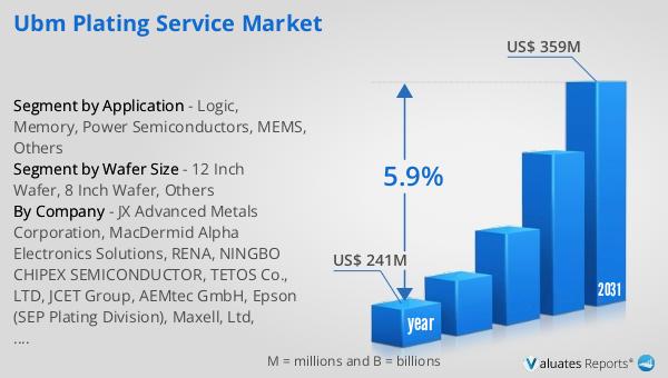
The global market for UBM Plating Service was valued at $241 million in 2024 and is anticipated to expand to a revised size of $359 million by 2031, reflecting a compound annual growth rate (CAGR) of 5.9% over the forecast period. This growth trajectory underscores the increasing demand for UBM plating services across various sectors, driven by the rapid advancements in semiconductor technology and the growing need for high-performance electronic devices. As industries such as consumer electronics, automotive, and telecommunications continue to evolve, the demand for more efficient and reliable semiconductor packaging solutions is expected to rise, further fueling the growth of the UBM plating service market. Companies operating in this market are likely to focus on enhancing their service offerings and expanding their capabilities to meet the diverse needs of their customers. This may involve investing in new technologies, improving process efficiencies, and developing innovative plating techniques to stay competitive in the market. Additionally, the growing emphasis on sustainability and environmental responsibility is expected to influence the development of new plating processes that minimize waste and reduce the environmental impact of semiconductor manufacturing. As the market continues to grow, companies that can effectively address these challenges and capitalize on emerging opportunities are likely to succeed in the competitive landscape of the Global UBM Plating Service Market.
| Report Metric | Details |
| Report Name | UBM Plating Service Market |
| Accounted market size in year | US$ 241 million |
| Forecasted market size in 2031 | US$ 359 million |
| CAGR | 5.9% |
| Base Year | year |
| Forecasted years | 2025 - 2031 |
| Segment by Wafer Size |
|
| Segment by Application |
|
| By Region |
|
| By Company | JX Advanced Metals Corporation, MacDermid Alpha Electronics Solutions, RENA, NINGBO CHIPEX SEMICONDUCTOR, TETOS Co., LTD, JCET Group, AEMtec GmbH, Epson (SEP Plating Division), Maxell, Ltd, PacTech, Uyemura, Advafab, Fraunhofer ISIT, AEMtec |
| Forecast units | USD million in value |
| Report coverage | Revenue and volume forecast, company share, competitive landscape, growth factors and trends |


