What is Global SiC Semiconductor Processing Equipment Market?
The Global SiC Semiconductor Processing Equipment Market refers to the worldwide industry focused on the manufacturing and distribution of equipment used in the production of silicon carbide (SiC) semiconductors. SiC semiconductors are known for their superior performance in high-temperature and high-voltage applications, making them ideal for use in power electronics, automotive, and renewable energy sectors. The market encompasses a range of equipment types, including crystal growth furnaces, cutting machines, epitaxy tools, and more, each playing a crucial role in the fabrication of SiC wafers and devices. As industries increasingly demand more efficient and durable semiconductor materials, the SiC processing equipment market is experiencing significant growth. This growth is driven by the need for advanced technologies that can support the production of high-quality SiC semiconductors, which are essential for the development of next-generation electronic devices. The market's expansion is further fueled by ongoing research and development efforts aimed at improving the efficiency and cost-effectiveness of SiC semiconductor manufacturing processes. As a result, the Global SiC Semiconductor Processing Equipment Market is poised to play a pivotal role in the future of electronics manufacturing.
SiC Crystal Growth Furnace, SiC Cutting Equipment, SiC Epitaxy/HTCVD Equipment, SiC Grinding/CMP Equipment, SiC Deposition Equipment, SiC Thermal Processing Equipment, SiC Etch and Clean Equipment, SiC Ion Implant Equipment, SiC Patterning Equipment, SiC Metrology and Inspection Equipment, SiC Wafer Bonders, Others in the Global SiC Semiconductor Processing Equipment Market:
The SiC Crystal Growth Furnace is a critical component in the production of silicon carbide semiconductors. It is used to grow high-quality SiC crystals, which serve as the foundation for all subsequent processing steps. This equipment operates under high temperatures and controlled environments to ensure the purity and structural integrity of the crystals. SiC Cutting Equipment is employed to slice the grown crystals into wafers, which are thin, flat pieces of semiconductor material. Precision is key in this process to minimize material waste and ensure uniformity in wafer thickness. SiC Epitaxy/HTCVD Equipment is used to deposit thin layers of silicon carbide onto the wafers, a process that enhances the electrical properties of the material. This step is crucial for tailoring the semiconductor's characteristics to specific applications. SiC Grinding/CMP Equipment is utilized to polish the wafer surfaces, ensuring they are smooth and defect-free. This is important for subsequent processing steps and for the overall performance of the final semiconductor devices. SiC Deposition Equipment is used to apply additional layers of materials onto the wafers, which can include metals or insulators, depending on the desired device structure. SiC Thermal Processing Equipment is involved in various heat treatments that modify the material properties of the wafers, such as annealing or oxidation. These processes are essential for activating dopants or forming protective layers. SiC Etch and Clean Equipment is used to pattern the wafers and remove unwanted material, a step that defines the intricate features of semiconductor devices. SiC Ion Implant Equipment introduces dopants into the wafer to modify its electrical properties, a critical step in creating p-n junctions and other device structures. SiC Patterning Equipment is used to create the detailed patterns required for complex semiconductor devices, often using photolithography techniques. SiC Metrology and Inspection Equipment ensures the quality and consistency of the wafers and devices by measuring various parameters and identifying defects. SiC Wafer Bonders are used to join wafers together, a process that can be important for creating multi-layered devices. Other equipment in the market may include specialized tools for specific applications or emerging technologies. Each piece of equipment plays a vital role in the intricate process of manufacturing SiC semiconductors, contributing to the overall efficiency and quality of the final products.
Silicon Carbide Wafer, Silicon Carbide Epitaxial Wafer, Silicon Carbide Devices in the Global SiC Semiconductor Processing Equipment Market:
The Global SiC Semiconductor Processing Equipment Market finds its usage in several key areas, including Silicon Carbide Wafer, Silicon Carbide Epitaxial Wafer, and Silicon Carbide Devices. Silicon Carbide Wafers are the foundational material upon which all SiC semiconductor devices are built. The processing equipment used in this area includes crystal growth furnaces, cutting machines, and grinding tools, all of which are essential for producing high-quality wafers. These wafers are characterized by their ability to withstand high temperatures and voltages, making them ideal for power electronics applications. Silicon Carbide Epitaxial Wafers are an advanced form of SiC wafers that have undergone an epitaxial growth process. This process involves depositing a thin layer of silicon carbide onto the wafer surface, enhancing its electrical properties. Epitaxy equipment, such as HTCVD tools, is crucial in this area, as it allows for precise control over the thickness and composition of the epitaxial layer. This results in wafers that are tailored for specific applications, such as high-frequency or high-power devices. Silicon Carbide Devices are the end products of the SiC semiconductor manufacturing process. These devices, which include diodes, transistors, and integrated circuits, benefit from the superior properties of SiC, such as high thermal conductivity and breakdown voltage. The processing equipment used in this area includes deposition tools, etching machines, and ion implantation systems, all of which contribute to the fabrication of complex device structures. The ability to produce reliable and efficient SiC devices is critical for industries such as automotive, renewable energy, and telecommunications, where performance and durability are paramount. Overall, the Global SiC Semiconductor Processing Equipment Market plays a vital role in enabling the production of high-performance SiC wafers and devices, driving innovation and growth in various high-tech sectors.
Global SiC Semiconductor Processing Equipment Market Outlook:
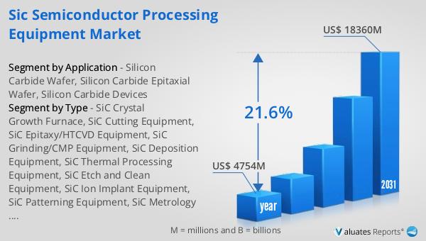
The global market for SiC Semiconductor Processing Equipment was valued at approximately $4,754 million in 2024. This market is anticipated to undergo significant growth, reaching an estimated size of $18,360 million by the year 2031. This expansion represents a compound annual growth rate (CAGR) of 21.6% over the forecast period. This impressive growth trajectory underscores the increasing demand for SiC semiconductors, driven by their superior performance in high-temperature and high-voltage applications. As industries such as automotive, renewable energy, and telecommunications continue to seek more efficient and durable semiconductor materials, the demand for SiC processing equipment is expected to rise. The market's growth is further supported by ongoing advancements in SiC manufacturing technologies, which are enhancing the efficiency and cost-effectiveness of semiconductor production. As a result, the Global SiC Semiconductor Processing Equipment Market is poised to play a crucial role in the future of electronics manufacturing, providing the tools necessary to produce the next generation of high-performance semiconductor devices. This growth not only reflects the increasing adoption of SiC technology but also highlights the market's potential to drive innovation and development across various high-tech industries.
| Report Metric | Details |
| Report Name | SiC Semiconductor Processing Equipment Market |
| Accounted market size in year | US$ 4754 million |
| Forecasted market size in 2031 | US$ 18360 million |
| CAGR | 21.6% |
| Base Year | year |
| Forecasted years | 2025 - 2031 |
| Segment by Type |
|
| Segment by Application |
|
| By Region |
|
| By Company | Applied Materials, Lam Research, Mattson Technology, Inc., SPTS Technologies, Oxford Instruments, Trymax Semiconductor, SCREEN Semiconductor, Tokyo Electron Ltd (TEL), ULVAC, Panasonic, Axcelis, Ion Beam Services (IBS), Kokusai Electric, Nissin Ion Equipment USA, Inc, Sumitomo Heavy Industries, Ltd., PR Hoffman, Inc., Revasum, Logitech, DISCO, TOKYO SEIMITSU (ACCRETECH), Okamoto Machine Tool Works, Ltd., KLA Corporation, Onto Innovation, Semilab, Camtek, Unity Semiconductor SAS, PVA TePla, Lasertec, Veeco, Aixtron, Thermco Systems Limited, ASM International NV, NuFlare Technology, Inc., Naura, GMC Semitech Co.,Ltd, Kingstone Semiconductor, Hwatsing Technology, Angkun Vision (Beijing) Technology, Shanghai Bangxin Semi Technology, Jingsheng Electromechanical, CETC 48, Engis, Wolfspeed, SiCrystal, II-VI Advanced Materials, TankeBlue, Takatori, Meyer Burger, Komatsu NTC |
| Forecast units | USD million in value |
| Report coverage | Revenue and volume forecast, company share, competitive landscape, growth factors and trends |


