What is Global SiC & GaN Wafer Cleaning Equipment Market?
The Global SiC & GaN Wafer Cleaning Equipment Market refers to the industry focused on the production and sale of equipment used to clean silicon carbide (SiC) and gallium nitride (GaN) wafers. These wafers are essential components in the semiconductor industry, used in the manufacturing of electronic devices. Cleaning these wafers is a critical step in the production process, as it ensures the removal of contaminants that could affect the performance and reliability of the final product. The market for this equipment is driven by the increasing demand for high-performance electronic devices, which require advanced materials like SiC and GaN. These materials are favored for their superior electrical properties, which enable the production of more efficient and powerful devices. As the demand for such devices grows, so does the need for effective wafer cleaning solutions, making this market an important segment of the semiconductor industry.
Single Wafer Cleaning Equipment, Batch Wafer Cleaning Equipment in the Global SiC & GaN Wafer Cleaning Equipment Market:
Single Wafer Cleaning Equipment and Batch Wafer Cleaning Equipment are two primary types of cleaning solutions used in the Global SiC & GaN Wafer Cleaning Equipment Market. Single Wafer Cleaning Equipment is designed to clean one wafer at a time, providing a high level of precision and control. This type of equipment is particularly useful in applications where the highest level of cleanliness is required, as it allows for meticulous attention to each individual wafer. The process typically involves a series of steps, including chemical cleaning, rinsing, and drying, all of which are carefully controlled to ensure optimal results. This method is often preferred for high-value wafers or those used in critical applications, where even the smallest defect could lead to significant performance issues. On the other hand, Batch Wafer Cleaning Equipment is designed to clean multiple wafers simultaneously. This approach is more efficient in terms of throughput, as it allows for the processing of a large number of wafers in a single cycle. Batch cleaning is generally used in high-volume manufacturing environments, where speed and efficiency are paramount. The process involves immersing a batch of wafers in a series of chemical baths, followed by rinsing and drying. While this method may not offer the same level of precision as single wafer cleaning, it is highly effective for applications where large quantities of wafers need to be processed quickly. Both types of equipment play a crucial role in the semiconductor manufacturing process, ensuring that wafers are free from contaminants that could compromise the performance of the final product. The choice between single and batch wafer cleaning equipment often depends on the specific requirements of the manufacturing process, including factors such as volume, precision, and cost. As the demand for SiC and GaN wafers continues to grow, driven by the increasing need for high-performance electronic devices, the market for both single and batch wafer cleaning equipment is expected to expand, offering a range of solutions to meet the diverse needs of the semiconductor industry.
SiC Power Devices, GaN Semiconductor Devices in the Global SiC & GaN Wafer Cleaning Equipment Market:
The Global SiC & GaN Wafer Cleaning Equipment Market plays a vital role in the production of SiC Power Devices and GaN Semiconductor Devices, both of which are essential components in modern electronics. SiC Power Devices are used in a variety of applications, including power converters, inverters, and motor drives, where they offer significant advantages over traditional silicon-based devices. These advantages include higher efficiency, faster switching speeds, and the ability to operate at higher temperatures, making them ideal for use in demanding environments such as electric vehicles and renewable energy systems. The cleaning of SiC wafers is a critical step in the manufacturing process, as any contaminants left on the wafer surface can lead to defects that affect the performance and reliability of the final device. GaN Semiconductor Devices, on the other hand, are used in applications such as radio frequency amplifiers, light-emitting diodes (LEDs), and power electronics. GaN devices are known for their high electron mobility, which allows for faster operation and greater efficiency compared to silicon-based devices. The cleaning of GaN wafers is equally important, as it ensures the removal of impurities that could impact the device's performance. In both cases, the use of advanced wafer cleaning equipment is essential to achieving the high levels of cleanliness required for these cutting-edge devices. The Global SiC & GaN Wafer Cleaning Equipment Market provides the tools and technologies needed to meet these stringent requirements, supporting the production of high-quality SiC and GaN devices that are critical to the advancement of modern electronics. As the demand for these devices continues to grow, driven by the increasing need for more efficient and powerful electronic systems, the importance of effective wafer cleaning solutions will only continue to increase.
Global SiC & GaN Wafer Cleaning Equipment Market Outlook:
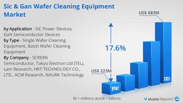
In 2024, the global market for SiC and GaN Wafer Cleaning Equipment was valued at approximately $223 million. This market is anticipated to experience significant growth, reaching an estimated size of $683 million by 2031. This growth trajectory represents a compound annual growth rate (CAGR) of 17.6% over the forecast period. This impressive expansion is indicative of the increasing demand for SiC and GaN wafers, driven by their superior performance characteristics in electronic devices. As industries continue to seek more efficient and powerful components, the need for high-quality wafer cleaning equipment becomes more pronounced. The projected growth in this market underscores the critical role that wafer cleaning equipment plays in the semiconductor manufacturing process, ensuring that wafers are free from contaminants that could compromise device performance. This market outlook highlights the importance of investing in advanced cleaning technologies to support the production of next-generation electronic devices. As the industry evolves, the demand for SiC and GaN wafers is expected to rise, further fueling the need for effective cleaning solutions. The growth of this market reflects the broader trends in the semiconductor industry, where innovation and efficiency are key drivers of success.
| Report Metric | Details |
| Report Name | SiC & GaN Wafer Cleaning Equipment Market |
| Accounted market size in year | US$ 223 million |
| Forecasted market size in 2031 | US$ 683 million |
| CAGR | 17.6% |
| Base Year | year |
| Forecasted years | 2025 - 2031 |
| by Type |
|
| by Application |
|
| Production by Region |
|
| Consumption by Region |
|
| By Company | SCREEN Semiconductor, Tokyo Electron Ltd (TEL), Lam Research, HRT TECHNOLOGY CO., LTD., ACM Research, NAURA Technology |
| Forecast units | USD million in value |
| Report coverage | Revenue and volume forecast, company share, competitive landscape, growth factors and trends |


