What is Global CD-SEM Metrology Systems Market?
The Global CD-SEM Metrology Systems Market is a specialized segment within the semiconductor industry that focuses on the use of Critical Dimension Scanning Electron Microscopes (CD-SEM) for precise measurement and analysis of semiconductor wafers. These systems are crucial for ensuring the quality and performance of semiconductor devices by providing accurate measurements of the critical dimensions of various features on a wafer. As the demand for smaller, more efficient, and powerful electronic devices grows, the need for advanced metrology systems like CD-SEM becomes increasingly important. These systems help manufacturers maintain tight control over the production process, ensuring that each component meets the necessary specifications. The market for CD-SEM metrology systems is driven by the continuous advancements in semiconductor technology, which require ever-more precise measurement capabilities. Additionally, the increasing complexity of semiconductor devices, with their smaller geometries and higher densities, further fuels the demand for these sophisticated metrology tools. As a result, the Global CD-SEM Metrology Systems Market is poised for significant growth, driven by the ongoing evolution of the semiconductor industry and the relentless pursuit of technological innovation.
High Resolution, Low Resolution in the Global CD-SEM Metrology Systems Market:
In the realm of Global CD-SEM Metrology Systems, resolution plays a pivotal role in determining the accuracy and precision of measurements. High-resolution CD-SEM systems are designed to provide extremely detailed images and measurements of semiconductor wafers, allowing for the detection of even the smallest defects and variations in critical dimensions. These systems are essential for advanced semiconductor manufacturing processes, where the margin for error is minimal, and the demand for precision is paramount. High-resolution systems are typically used in the production of cutting-edge semiconductor devices, such as those found in high-performance computing, telecommunications, and consumer electronics. They enable manufacturers to achieve the tight tolerances required for the latest generation of chips, ensuring optimal performance and reliability. On the other hand, low-resolution CD-SEM systems offer a more cost-effective solution for applications where ultra-high precision is not as critical. These systems are often used in less demanding manufacturing processes or for quality control purposes, where the primary goal is to ensure that the overall dimensions of a wafer meet the required specifications. While they may not provide the same level of detail as high-resolution systems, low-resolution CD-SEM systems still play a vital role in the semiconductor manufacturing process by offering a balance between cost and performance. The choice between high-resolution and low-resolution CD-SEM systems ultimately depends on the specific requirements of the manufacturing process and the desired level of precision. As semiconductor technology continues to advance, the demand for both high-resolution and low-resolution CD-SEM systems is expected to grow, driven by the need for increasingly sophisticated metrology solutions. Manufacturers must carefully consider their specific needs and budget constraints when selecting the appropriate CD-SEM system for their operations. By doing so, they can ensure that they are equipped with the right tools to meet the challenges of modern semiconductor manufacturing and maintain a competitive edge in the rapidly evolving global market.
300 mm Wafer, 200 mm Wafer, Others in the Global CD-SEM Metrology Systems Market:
The Global CD-SEM Metrology Systems Market finds its application in various areas, including the measurement and analysis of 300 mm wafers, 200 mm wafers, and other semiconductor substrates. The 300 mm wafer segment represents a significant portion of the market, as these larger wafers are commonly used in the production of advanced semiconductor devices. The increased surface area of 300 mm wafers allows for the production of more chips per wafer, leading to greater efficiency and cost savings for manufacturers. CD-SEM metrology systems are essential for ensuring the quality and precision of these larger wafers, as they provide the detailed measurements needed to maintain tight control over the manufacturing process. In contrast, 200 mm wafers are typically used in the production of less advanced semiconductor devices, such as those found in automotive and industrial applications. While the demand for 200 mm wafers has decreased in recent years due to the shift towards larger wafer sizes, they still play a crucial role in the semiconductor industry. CD-SEM metrology systems are used to ensure the quality and performance of 200 mm wafers, providing the necessary measurements to maintain the required specifications. Additionally, the Global CD-SEM Metrology Systems Market also encompasses other semiconductor substrates, such as those used in the production of specialized devices like sensors and MEMS (Micro-Electro-Mechanical Systems). These substrates often require unique measurement capabilities, and CD-SEM systems are well-suited to meet these needs. By providing accurate and reliable measurements, CD-SEM metrology systems help manufacturers maintain the quality and performance of their products, regardless of the specific substrate being used. As the semiconductor industry continues to evolve, the demand for CD-SEM metrology systems across all wafer sizes and substrates is expected to grow, driven by the need for increasingly precise and reliable measurement solutions.
Global CD-SEM Metrology Systems Market Outlook:
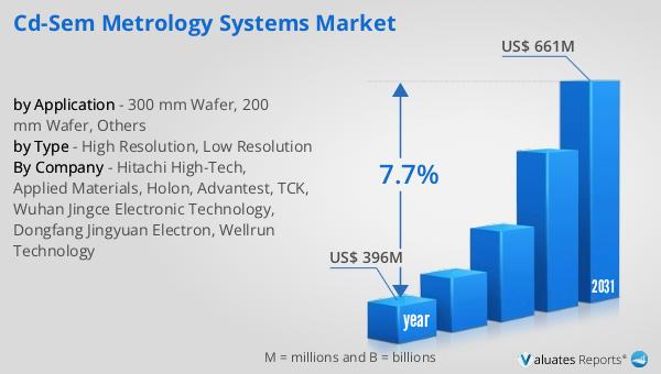
The outlook for the Global CD-SEM Metrology Systems Market is promising, with significant growth anticipated over the coming years. In 2024, the market was valued at approximately US$ 396 million, reflecting the strong demand for advanced metrology solutions in the semiconductor industry. As technology continues to advance and the need for smaller, more efficient electronic devices grows, the demand for CD-SEM systems is expected to increase. By 2031, the market is projected to reach a revised size of US$ 661 million, representing a compound annual growth rate (CAGR) of 7.7% during the forecast period. This growth is driven by the ongoing advancements in semiconductor technology, which require increasingly precise measurement capabilities to ensure the quality and performance of semiconductor devices. The increasing complexity of semiconductor devices, with their smaller geometries and higher densities, further fuels the demand for sophisticated metrology tools like CD-SEM systems. As manufacturers strive to maintain tight control over the production process and meet the ever-growing demand for advanced electronic devices, the Global CD-SEM Metrology Systems Market is poised for significant expansion. This growth presents numerous opportunities for manufacturers and suppliers of CD-SEM systems, as they work to develop and deliver the cutting-edge solutions needed to support the evolving needs of the semiconductor industry.
| Report Metric | Details |
| Report Name | CD-SEM Metrology Systems Market |
| Accounted market size in year | US$ 396 million |
| Forecasted market size in 2031 | US$ 661 million |
| CAGR | 7.7% |
| Base Year | year |
| Forecasted years | 2025 - 2031 |
| by Type |
|
| by Application |
|
| Production by Region |
|
| Consumption by Region |
|
| By Company | Hitachi High-Tech, Applied Materials, Holon, Advantest, TCK, Wuhan Jingce Electronic Technology, Dongfang Jingyuan Electron, Wellrun Technology |
| Forecast units | USD million in value |
| Report coverage | Revenue and volume forecast, company share, competitive landscape, growth factors and trends |


