What is Global GaN Inspection and Metrology Equipment Market?
The Global GaN Inspection and Metrology Equipment Market is a specialized segment within the semiconductor industry that focuses on the tools and technologies used to inspect and measure Gallium Nitride (GaN) materials and devices. GaN is a semiconductor material that has gained significant attention due to its superior properties, such as high electron mobility, high thermal conductivity, and wide bandgap, which make it ideal for high-power and high-frequency applications. The market for GaN inspection and metrology equipment is driven by the increasing demand for GaN-based devices in various industries, including telecommunications, automotive, and consumer electronics. These devices require precise inspection and measurement to ensure quality and performance, which is where GaN inspection and metrology equipment come into play. The equipment used in this market includes advanced tools that can detect defects, measure dimensions, and analyze the properties of GaN materials and devices. As the demand for GaN-based technologies continues to grow, the market for inspection and metrology equipment is expected to expand, providing opportunities for manufacturers and suppliers in this niche industry.
GaN Defect Inspection Equipment, GaN Metrology Equipment in the Global GaN Inspection and Metrology Equipment Market:
GaN Defect Inspection Equipment is a crucial component of the Global GaN Inspection and Metrology Equipment Market. This equipment is designed to identify and analyze defects in GaN materials and devices, which is essential for ensuring the quality and reliability of GaN-based products. Defects in GaN can significantly impact the performance and efficiency of devices, making defect inspection a critical step in the manufacturing process. GaN defect inspection equipment utilizes advanced technologies such as optical inspection, X-ray inspection, and electron microscopy to detect and characterize defects at various stages of production. These tools are capable of identifying a wide range of defects, including dislocations, voids, and surface irregularities, which can affect the electrical and thermal properties of GaN devices. By providing detailed information about the nature and location of defects, GaN defect inspection equipment helps manufacturers improve their production processes and enhance the quality of their products. On the other hand, GaN Metrology Equipment is focused on measuring the physical and electrical properties of GaN materials and devices. This equipment is used to ensure that GaN products meet the required specifications and performance standards. GaN metrology equipment includes tools for measuring parameters such as thickness, roughness, and electrical conductivity, which are critical for the performance of GaN-based devices. These measurements are essential for optimizing the design and manufacturing processes of GaN products, as they provide valuable insights into the material properties and device performance. GaN metrology equipment also plays a vital role in research and development, as it enables scientists and engineers to study the properties of GaN materials and develop new applications and technologies. The combination of defect inspection and metrology equipment provides a comprehensive solution for the quality control and assurance of GaN-based products, ensuring that they meet the high standards required for advanced applications. As the demand for GaN technologies continues to grow, the market for GaN defect inspection and metrology equipment is expected to expand, driven by the need for high-quality and reliable GaN products.
GaN RF, GaN Power, HB GaN LED in the Global GaN Inspection and Metrology Equipment Market:
The Global GaN Inspection and Metrology Equipment Market plays a significant role in various applications, including GaN RF, GaN Power, and HB GaN LED. In the GaN RF (Radio Frequency) sector, GaN materials are used to produce high-frequency devices that are essential for wireless communication systems, radar, and satellite communications. The inspection and metrology equipment in this area ensures that GaN RF devices meet the stringent performance and reliability standards required for these applications. By detecting defects and measuring critical parameters, the equipment helps manufacturers produce high-quality GaN RF devices that offer superior performance and efficiency. In the GaN Power sector, GaN materials are used to develop power devices that are more efficient and compact than traditional silicon-based devices. These devices are used in various applications, including power converters, inverters, and motor drives. The inspection and metrology equipment in this sector ensures that GaN power devices meet the required specifications and performance standards, enabling manufacturers to produce reliable and efficient products. By providing detailed information about the material properties and device performance, the equipment helps optimize the design and manufacturing processes of GaN power devices. In the HB GaN LED (High Brightness Gallium Nitride Light Emitting Diode) sector, GaN materials are used to produce high-brightness LEDs that are used in various lighting applications, including automotive lighting, display backlighting, and general illumination. The inspection and metrology equipment in this area ensures that HB GaN LEDs meet the required quality and performance standards, enabling manufacturers to produce high-quality and reliable products. By detecting defects and measuring critical parameters, the equipment helps optimize the production processes of HB GaN LEDs, ensuring that they offer superior brightness and efficiency. Overall, the Global GaN Inspection and Metrology Equipment Market plays a crucial role in ensuring the quality and reliability of GaN-based products across various applications, driving the growth and adoption of GaN technologies in different industries.
Global GaN Inspection and Metrology Equipment Market Outlook:
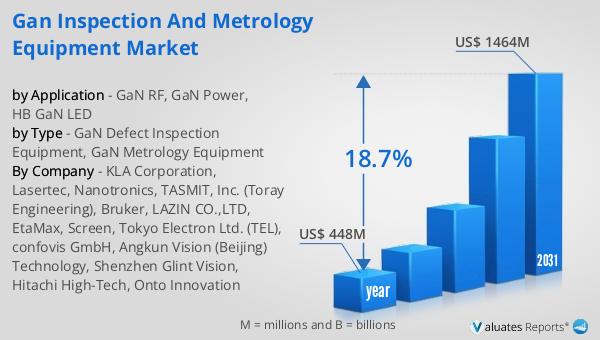
The global market for GaN Inspection and Metrology Equipment was valued at $448 million in 2024 and is anticipated to grow significantly, reaching an estimated size of $1,464 million by 2031. This growth represents a compound annual growth rate (CAGR) of 18.7% over the forecast period. This impressive growth trajectory underscores the increasing demand for GaN-based technologies across various industries, including telecommunications, automotive, and consumer electronics. As GaN materials continue to gain popularity due to their superior properties, the need for precise inspection and measurement tools becomes more critical. The market's expansion is driven by the growing adoption of GaN devices, which require high-quality inspection and metrology equipment to ensure their performance and reliability. Manufacturers and suppliers in the GaN Inspection and Metrology Equipment Market are poised to benefit from this growth, as they provide the essential tools and technologies needed to support the development and production of GaN-based products. The market's robust growth prospects highlight the importance of GaN technologies in the future of the semiconductor industry, as they offer significant advantages over traditional materials in terms of performance, efficiency, and reliability.
| Report Metric | Details |
| Report Name | GaN Inspection and Metrology Equipment Market |
| Accounted market size in year | US$ 448 million |
| Forecasted market size in 2031 | US$ 1464 million |
| CAGR | 18.7% |
| Base Year | year |
| Forecasted years | 2025 - 2031 |
| by Type |
|
| by Application |
|
| Production by Region |
|
| Consumption by Region |
|
| By Company | KLA Corporation, Lasertec, Nanotronics, TASMIT, Inc. (Toray Engineering), Bruker, LAZIN CO.,LTD, EtaMax, Screen, Tokyo Electron Ltd. (TEL), confovis GmbH, Angkun Vision (Beijing) Technology, Shenzhen Glint Vision, Hitachi High-Tech, Onto Innovation |
| Forecast units | USD million in value |
| Report coverage | Revenue and volume forecast, company share, competitive landscape, growth factors and trends |


