What is Global Etching Equipment for Compound Semiconductors Market?
The Global Etching Equipment for Compound Semiconductors Market is a specialized segment within the semiconductor industry that focuses on the tools and machinery used to etch or pattern compound semiconductor materials. Compound semiconductors, such as silicon carbide (SiC), gallium nitride (GaN), gallium arsenide (GaAs), and indium phosphide (InP), are essential for producing high-performance electronic devices. These materials offer superior properties like higher electron mobility, thermal stability, and efficiency compared to traditional silicon semiconductors. Etching equipment is crucial in the manufacturing process as it helps define the intricate patterns and structures on semiconductor wafers, which are necessary for device functionality. The market for this equipment is driven by the increasing demand for advanced electronic devices, including power electronics, RF communication devices, and optoelectronics. As technology continues to evolve, the need for precise and efficient etching solutions becomes more critical, making this market an integral part of the semiconductor manufacturing ecosystem. The growth of this market is further fueled by the expanding applications of compound semiconductors in various industries, including automotive, telecommunications, and consumer electronics, highlighting its significance in the global technology landscape.
ICP Etching Equipment, CCP Etching Equipment in the Global Etching Equipment for Compound Semiconductors Market:
ICP (Inductively Coupled Plasma) Etching Equipment and CCP (Capacitively Coupled Plasma) Etching Equipment are two primary technologies used in the Global Etching Equipment for Compound Semiconductors Market. ICP etching equipment utilizes inductively coupled plasma to achieve high-density plasma generation, which is essential for etching complex patterns with high precision. This technology is particularly advantageous for applications requiring deep etching and high aspect ratio structures, making it suitable for advanced semiconductor devices. ICP etching offers excellent control over etch profiles and selectivity, allowing manufacturers to achieve the desired etching results with minimal damage to the underlying materials. On the other hand, CCP etching equipment employs capacitively coupled plasma, which is known for its simplicity and cost-effectiveness. CCP etching is typically used for less demanding applications where high precision is not as critical. It provides good uniformity and is often used for etching processes that require lower ion energy. Both ICP and CCP etching technologies play a vital role in the production of compound semiconductors, each catering to different requirements based on the complexity and precision needed for specific applications. The choice between ICP and CCP etching depends on factors such as the type of material being etched, the desired etch profile, and the specific application requirements. As the demand for compound semiconductors continues to grow, the need for advanced etching equipment that can deliver high precision and efficiency becomes increasingly important. Manufacturers are constantly innovating and improving these technologies to meet the evolving needs of the semiconductor industry. The development of new materials and the increasing complexity of semiconductor devices drive the demand for more sophisticated etching solutions. ICP and CCP etching equipment are at the forefront of this technological advancement, enabling the production of next-generation electronic devices. The global market for these etching technologies is expected to expand as industries such as telecommunications, automotive, and consumer electronics continue to adopt compound semiconductors for their superior performance characteristics. The ongoing research and development efforts in the field of etching technology are focused on enhancing the capabilities of ICP and CCP equipment, improving etch rates, selectivity, and uniformity, while reducing costs and environmental impact. As a result, the Global Etching Equipment for Compound Semiconductors Market is poised for significant growth, driven by the increasing demand for high-performance electronic devices and the continuous innovation in etching technology.
SiC Power Devices, GaN Devices, GaAs, and InP Devices in the Global Etching Equipment for Compound Semiconductors Market:
The usage of Global Etching Equipment for Compound Semiconductors Market is pivotal in several key areas, including SiC Power Devices, GaN Devices, GaAs, and InP Devices. SiC power devices are increasingly used in high-power and high-temperature applications due to their superior thermal conductivity and high breakdown voltage. Etching equipment is essential in the manufacturing of SiC devices, as it allows for precise patterning and structuring of the semiconductor material, which is crucial for the device's performance and reliability. GaN devices, known for their high electron mobility and efficiency, are widely used in RF communication and power conversion applications. The etching process for GaN devices requires high precision to achieve the desired electrical characteristics and device performance. ICP etching equipment is often preferred for GaN devices due to its ability to produce high aspect ratio structures with excellent control over etch profiles. GaAs devices are commonly used in optoelectronics and high-frequency applications, where their superior electron mobility and direct bandgap properties are advantageous. The etching process for GaAs devices involves creating intricate patterns and structures that are essential for the device's functionality. Both ICP and CCP etching equipment can be used for GaAs devices, depending on the specific requirements of the application. InP devices are primarily used in high-speed and high-frequency applications, such as fiber optic communications and microwave devices. The etching process for InP devices requires high precision and control to achieve the desired device characteristics. ICP etching equipment is often used for InP devices due to its ability to produce high-quality etch profiles with minimal damage to the material. The demand for etching equipment in these areas is driven by the increasing adoption of compound semiconductors in various industries, including telecommunications, automotive, and consumer electronics. As the demand for high-performance electronic devices continues to grow, the need for advanced etching solutions becomes more critical. The Global Etching Equipment for Compound Semiconductors Market plays a vital role in enabling the production of next-generation electronic devices, supporting the advancement of technology across multiple sectors.
Global Etching Equipment for Compound Semiconductors Market Outlook:
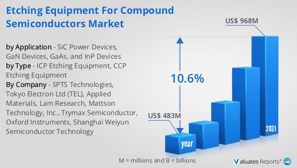
In 2024, the global market for Etching Equipment for Compound Semiconductors was valued at approximately $483 million. This market is anticipated to experience significant growth, reaching an estimated size of $968 million by 2031. This growth trajectory represents a compound annual growth rate (CAGR) of 10.6% over the forecast period. The expansion of this market is driven by the increasing demand for advanced electronic devices that utilize compound semiconductors, such as SiC, GaN, GaAs, and InP. These materials are essential for producing high-performance devices used in various applications, including power electronics, RF communication, and optoelectronics. The growing adoption of compound semiconductors in industries such as telecommunications, automotive, and consumer electronics further fuels the demand for etching equipment. As technology continues to evolve, the need for precise and efficient etching solutions becomes more critical, driving the growth of this market. The continuous innovation in etching technology, along with the development of new materials and the increasing complexity of semiconductor devices, contributes to the expansion of the Global Etching Equipment for Compound Semiconductors Market. This market is poised for significant growth, supported by the ongoing advancements in semiconductor manufacturing and the increasing demand for high-performance electronic devices.
| Report Metric | Details |
| Report Name | Etching Equipment for Compound Semiconductors Market |
| Accounted market size in year | US$ 483 million |
| Forecasted market size in 2031 | US$ 968 million |
| CAGR | 10.6% |
| Base Year | year |
| Forecasted years | 2025 - 2031 |
| by Type |
|
| by Application |
|
| Production by Region |
|
| Consumption by Region |
|
| By Company | SPTS Technologies, Tokyo Electron Ltd (TEL), Applied Materials, Lam Research, Mattson Technology, Inc., Trymax Semiconductor, Oxford Instruments, Shanghai Weiyun Semiconductor Technology |
| Forecast units | USD million in value |
| Report coverage | Revenue and volume forecast, company share, competitive landscape, growth factors and trends |


