What is Global SiC & GaN Wafer Defect Inspection System Market?
The Global SiC & GaN Wafer Defect Inspection System Market is a specialized segment within the semiconductor industry that focuses on the detection and analysis of defects in silicon carbide (SiC) and gallium nitride (GaN) wafers. These materials are crucial for the production of high-performance electronic devices, particularly in power electronics and RF applications. The inspection systems are designed to identify and categorize defects that can affect the performance and reliability of the final products. This market is driven by the increasing demand for SiC and GaN-based devices, which are known for their efficiency and ability to operate at higher temperatures and voltages compared to traditional silicon-based devices. As industries such as automotive, telecommunications, and renewable energy continue to grow, the need for high-quality SiC and GaN wafers becomes more critical, thereby fueling the demand for advanced defect inspection systems. These systems employ various technologies, including optical and X-ray inspection, to ensure that wafers meet stringent quality standards before they are used in device fabrication. The market is characterized by rapid technological advancements and a high level of competition among key players striving to offer more precise and efficient inspection solutions.
Optical Inspection System, X-ray Diffraction Imaging (XRDI) System in the Global SiC & GaN Wafer Defect Inspection System Market:
Optical Inspection Systems and X-ray Diffraction Imaging (XRDI) Systems are two pivotal technologies in the Global SiC & GaN Wafer Defect Inspection System Market. Optical Inspection Systems utilize advanced imaging techniques to detect surface defects on wafers. These systems are equipped with high-resolution cameras and sophisticated software algorithms that can identify even the smallest imperfections, such as scratches, pits, or particles, on the wafer surface. The primary advantage of optical inspection is its ability to provide real-time feedback, allowing manufacturers to quickly address any issues in the production process. This technology is particularly effective for inspecting large volumes of wafers, making it a preferred choice for high-throughput environments. On the other hand, X-ray Diffraction Imaging (XRDI) Systems offer a different approach by examining the internal structure of the wafers. XRDI is capable of detecting subsurface defects, such as dislocations or voids, that are not visible through optical inspection. This method involves directing X-rays onto the wafer and analyzing the diffraction patterns to identify any irregularities in the crystal structure. XRDI is highly valued for its ability to provide detailed insights into the material properties of SiC and GaN wafers, which is crucial for ensuring the performance and reliability of the final devices. While optical inspection is more commonly used due to its speed and efficiency, XRDI is often employed for more in-depth analysis when high precision is required. Both technologies play a complementary role in the defect inspection process, ensuring that wafers meet the necessary quality standards before they proceed to the next stages of device fabrication. As the demand for SiC and GaN-based devices continues to rise, manufacturers are increasingly investing in these advanced inspection systems to maintain competitive advantage and meet the stringent quality requirements of their customers.
SiC Substrate, Epitaxy and Devices, GaN Substrate, Epitaxy and Devices in the Global SiC & GaN Wafer Defect Inspection System Market:
The usage of Global SiC & GaN Wafer Defect Inspection Systems is critical in various stages of semiconductor manufacturing, particularly in the areas of SiC Substrate, Epitaxy, and Devices, as well as GaN Substrate, Epitaxy, and Devices. In the SiC substrate manufacturing process, defect inspection systems are employed to ensure that the raw wafers are free from surface and subsurface defects that could compromise the performance of the final devices. These systems help in identifying issues such as micropipes, dislocations, and other structural irregularities that can affect the electrical properties of the substrate. During the epitaxy process, where a thin layer of semiconductor material is grown on the substrate, defect inspection systems play a crucial role in monitoring the quality of the epitaxial layer. Any defects in this layer can lead to device failure or reduced efficiency, making inspection an essential step in the production process. Similarly, in the manufacturing of SiC devices, defect inspection systems are used to ensure that the devices meet the required specifications and are free from any defects that could impact their performance. For GaN substrates and devices, the inspection systems are equally important. GaN is known for its superior electronic properties, but it is also more prone to defects during the manufacturing process. Defect inspection systems help in identifying and mitigating these issues, ensuring that the GaN wafers and devices meet the high standards required for applications such as RF amplifiers and LED lighting. Overall, the use of defect inspection systems in these areas is vital for maintaining the quality and reliability of SiC and GaN-based products, which are increasingly in demand across various industries.
Global SiC & GaN Wafer Defect Inspection System Market Outlook:
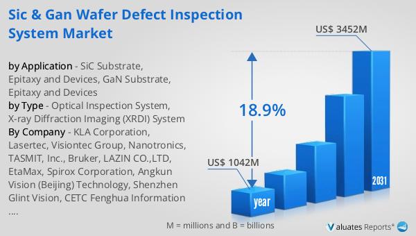
The global market for SiC and GaN Wafer Defect Inspection Systems was valued at approximately $1,042 million in 2024 and is anticipated to expand to around $3,452 million by 2031, reflecting a compound annual growth rate (CAGR) of 18.9% over the forecast period. The market is highly concentrated, with the top five players commanding about 95% of the market share. North America emerges as the largest regional market, accounting for roughly 32% of the total market share, followed by Europe and Japan, which hold shares of approximately 27% and 15%, respectively. In terms of product types, the Optical Inspection System dominates the market, capturing a significant share of 97%. This dominance is attributed to the system's efficiency and capability to handle large volumes of wafers, making it an indispensable tool in high-throughput manufacturing environments. The robust growth of this market is driven by the increasing demand for high-quality SiC and GaN wafers, which are essential for the production of advanced electronic devices used in various industries, including automotive, telecommunications, and renewable energy. As the market continues to evolve, manufacturers are focusing on enhancing the precision and efficiency of their inspection systems to meet the growing quality standards and maintain a competitive edge.
| Report Metric | Details |
| Report Name | SiC & GaN Wafer Defect Inspection System Market |
| Accounted market size in year | US$ 1042 million |
| Forecasted market size in 2031 | US$ 3452 million |
| CAGR | 18.9% |
| Base Year | year |
| Forecasted years | 2025 - 2031 |
| by Type |
|
| by Application |
|
| Production by Region |
|
| Consumption by Region |
|
| By Company | KLA Corporation, Lasertec, Visiontec Group, Nanotronics, TASMIT, Inc., Bruker, LAZIN CO.,LTD, EtaMax, Spirox Corporation, Angkun Vision (Beijing) Technology, Shenzhen Glint Vision, CETC Fenghua Information Equipment, CASI Vision Technology (Luoyang) Co., Ltd, Shanghai Youruipu Semiconductor Equipment, Dalian Chuangrui Spectral Technology Co., Ltd, T-Vision.AI (Hangzhou) Tech Co.,Ltd., HGTECH |
| Forecast units | USD million in value |
| Report coverage | Revenue and volume forecast, company share, competitive landscape, growth factors and trends |


