What is Global SiC & GaN Device Wafer Front-End Equipment Market?
The Global SiC & GaN Device Wafer Front-End Equipment Market refers to the industry that provides the essential machinery and tools required for the production of silicon carbide (SiC) and gallium nitride (GaN) semiconductor devices. These materials are crucial in the semiconductor industry due to their superior properties, such as high thermal conductivity, high breakdown voltage, and high electron mobility, which make them ideal for high-power and high-frequency applications. The market encompasses a wide range of equipment used in the initial stages of semiconductor device manufacturing, including epitaxy, etching, cleaning, ion implantation, annealing, oxidation, wafer thinning, chemical mechanical polishing (CMP), metrology, and inspection. As the demand for more efficient and powerful electronic devices grows, the need for advanced SiC and GaN devices also increases, driving the expansion of this market. The equipment used in this market is critical for ensuring the quality and performance of the final semiconductor products, making it a vital component of the global electronics supply chain. The market is characterized by rapid technological advancements and a high level of competition among key players striving to innovate and improve their offerings to meet the evolving needs of the semiconductor industry.
SiC & GaN Epitaxy Equipment, SiC & GaN Etch and Clean Equipment, SiC & GaN Ion Implanter, SiC & GaN Anneal and Oxidation Equipment, SiC & GaN Wafer Thinning/CMP Tools, SiC & GaN Metrology and Inspection Equipment in the Global SiC & GaN Device Wafer Front-End Equipment Market:
SiC & GaN Epitaxy Equipment is crucial in the Global SiC & GaN Device Wafer Front-End Equipment Market as it facilitates the growth of high-quality crystalline layers on substrates, which is essential for the performance of semiconductor devices. This equipment ensures that the epitaxial layers have the desired electrical properties and thickness, which are critical for device functionality. SiC & GaN Etch and Clean Equipment play a vital role in shaping and cleaning the wafer surfaces. Etching is used to create patterns on the wafer, while cleaning removes any contaminants that could affect device performance. These processes are essential for achieving the precision and cleanliness required in semiconductor manufacturing. SiC & GaN Ion Implanters are used to introduce dopants into the semiconductor material, altering its electrical properties to create p-type or n-type regions. This process is crucial for forming the active regions of semiconductor devices. SiC & GaN Anneal and Oxidation Equipment are used to repair damage caused by ion implantation and to grow oxide layers on the wafer surface, respectively. Annealing helps to activate dopants and improve the crystal quality, while oxidation is used to create insulating layers that are essential for device operation. SiC & GaN Wafer Thinning/CMP Tools are used to reduce the thickness of the wafers and to achieve a smooth surface finish. Thinning is important for improving heat dissipation and reducing the overall size of the devices, while CMP ensures that the wafer surface is flat and free of defects. SiC & GaN Metrology and Inspection Equipment are used to measure and inspect the wafers at various stages of the manufacturing process. These tools ensure that the wafers meet the required specifications and are free of defects, which is crucial for maintaining high yields and ensuring the reliability of the final devices. The Global SiC & GaN Device Wafer Front-End Equipment Market is driven by the increasing demand for high-performance semiconductor devices in various applications, including power electronics, telecommunications, and automotive. As the industry continues to evolve, manufacturers are investing in advanced equipment to improve the efficiency and quality of their production processes. This market is characterized by rapid technological advancements and a high level of competition among key players striving to innovate and improve their offerings to meet the evolving needs of the semiconductor industry.
SiC Semiconductor Devices, GaN Semiconductor Devices in the Global SiC & GaN Device Wafer Front-End Equipment Market:
The usage of Global SiC & GaN Device Wafer Front-End Equipment Market in SiC Semiconductor Devices is primarily driven by the need for high-performance power electronics. SiC devices are known for their ability to operate at higher temperatures, voltages, and frequencies compared to traditional silicon-based devices. This makes them ideal for applications in electric vehicles, renewable energy systems, and industrial power supplies. The equipment used in the front-end manufacturing of SiC devices ensures that the wafers have the necessary properties to withstand these demanding conditions. Epitaxy equipment is used to grow high-quality SiC layers, while etch and clean equipment ensure that the wafers are free of defects and contaminants. Ion implanters are used to introduce dopants into the SiC material, creating the necessary p-type and n-type regions for device operation. Anneal and oxidation equipment are used to repair implantation damage and to grow insulating oxide layers, which are essential for device functionality. Wafer thinning and CMP tools are used to reduce the thickness of the SiC wafers, improving heat dissipation and reducing the overall size of the devices. Metrology and inspection equipment are used to ensure that the wafers meet the required specifications and are free of defects, which is crucial for maintaining high yields and ensuring the reliability of the final devices. In GaN Semiconductor Devices, the usage of Global SiC & GaN Device Wafer Front-End Equipment Market is driven by the demand for high-frequency and high-power applications. GaN devices are known for their high electron mobility and high breakdown voltage, making them ideal for applications in RF amplifiers, wireless communication systems, and radar systems. The equipment used in the front-end manufacturing of GaN devices ensures that the wafers have the necessary properties to operate at these high frequencies and power levels. Epitaxy equipment is used to grow high-quality GaN layers, while etch and clean equipment ensure that the wafers are free of defects and contaminants. Ion implanters are used to introduce dopants into the GaN material, creating the necessary p-type and n-type regions for device operation. Anneal and oxidation equipment are used to repair implantation damage and to grow insulating oxide layers, which are essential for device functionality. Wafer thinning and CMP tools are used to reduce the thickness of the GaN wafers, improving heat dissipation and reducing the overall size of the devices. Metrology and inspection equipment are used to ensure that the wafers meet the required specifications and are free of defects, which is crucial for maintaining high yields and ensuring the reliability of the final devices. The Global SiC & GaN Device Wafer Front-End Equipment Market is essential for the production of high-performance SiC and GaN semiconductor devices, which are increasingly being used in a wide range of applications due to their superior properties.
Global SiC & GaN Device Wafer Front-End Equipment Market Outlook:
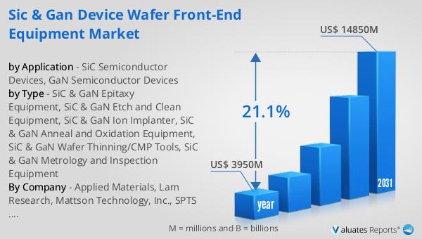
In 2024, the worldwide market for SiC and GaN Device Wafer Front-End Equipment was estimated to be worth approximately $3.95 billion. This market is anticipated to expand significantly, reaching an adjusted valuation of around $14.85 billion by 2031. This growth trajectory represents a compound annual growth rate (CAGR) of 21.1% throughout the forecast period. The substantial increase in market size underscores the growing demand for SiC and GaN devices, driven by their superior performance characteristics in high-power and high-frequency applications. As industries such as automotive, telecommunications, and renewable energy increasingly adopt these advanced semiconductor materials, the need for specialized front-end equipment to manufacture these devices is expected to rise. The market's expansion is also fueled by ongoing technological advancements and innovations in equipment design, which enhance the efficiency and quality of the manufacturing process. Companies operating in this space are likely to focus on developing cutting-edge solutions to meet the evolving needs of the semiconductor industry, thereby contributing to the market's robust growth. This dynamic market environment presents significant opportunities for both established players and new entrants looking to capitalize on the increasing demand for SiC and GaN device wafer front-end equipment.
| Report Metric | Details |
| Report Name | SiC & GaN Device Wafer Front-End Equipment Market |
| Accounted market size in year | US$ 3950 million |
| Forecasted market size in 2031 | US$ 14850 million |
| CAGR | 21.1% |
| Base Year | year |
| Forecasted years | 2025 - 2031 |
| by Type |
|
| by Application |
|
| Production by Region |
|
| Consumption by Region |
|
| By Company | Applied Materials, Lam Research, Mattson Technology, Inc., SPTS Technologies, Oxford Instruments, Trymax Semiconductor, SCREEN Semiconductor, Tokyo Electron Ltd (TEL), ULVAC, Panasonic, Axcelis, Ion Beam Services (IBS), Kokusai Electric, Nissin Ion Equipment USA, Inc, Sumitomo Heavy Industries, Ltd., PR Hoffman, Inc., Revasum, Logitech, DISCO, TOKYO SEIMITSU (ACCRETECH), Okamoto Machine Tool Works, Ltd., KLA Corporation, Onto Innovation, Semilab, Camtek, Unity Semiconductor SAS, PVA TePla, Lasertec, Veeco, Aixtron, Thermco Systems Limited, ASM International NV, NuFlare Technology, Inc., Naura, GMC Semitech Co.,Ltd, Kingstone Semiconductor, Hwatsing Technology, Angkun Vision (Beijing) Technology, Shanghai Bangxin Semi Technology, Jingsheng Electromechanical, CETC 48 |
| Forecast units | USD million in value |
| Report coverage | Revenue and volume forecast, company share, competitive landscape, growth factors and trends |


