Wednesday, March 5, 2025

Global Medical Thermistor Market Research Report 2025

What is Global Medical Thermistor Market?

The Global Medical Thermistor Market is a specialized segment within the broader medical device industry, focusing on thermistors used in various medical applications. Thermistors are temperature-sensitive resistors that change resistance with temperature changes, making them ideal for precise temperature monitoring and control. In the medical field, these devices are crucial for applications such as patient monitoring, diagnostic equipment, and therapeutic devices. The market is driven by the increasing demand for advanced healthcare solutions, the growing prevalence of chronic diseases, and the need for accurate temperature measurement in medical procedures. As healthcare technology advances, the demand for reliable and efficient thermistors continues to grow, contributing to the expansion of the global medical thermistor market. The market is characterized by continuous innovation and development, with manufacturers focusing on enhancing the accuracy, reliability, and miniaturization of thermistors to meet the evolving needs of the healthcare industry. Overall, the Global Medical Thermistor Market plays a vital role in ensuring the safety and effectiveness of medical devices, ultimately improving patient outcomes and advancing healthcare delivery worldwide.

Medical Thermistor Market

NTC Thermistor, PTC Thermistor in the Global Medical Thermistor Market:

NTC (Negative Temperature Coefficient) and PTC (Positive Temperature Coefficient) thermistors are two primary types of thermistors used in the Global Medical Thermistor Market, each serving distinct purposes based on their unique properties. NTC thermistors decrease in resistance as temperature increases, making them highly sensitive and suitable for precise temperature measurements. They are commonly used in medical applications where accurate temperature monitoring is critical, such as in patient monitoring systems, incubators, and respiratory devices. The ability of NTC thermistors to provide rapid and accurate temperature readings makes them indispensable in situations where even slight temperature variations can have significant impacts on patient care and treatment outcomes. On the other hand, PTC thermistors increase in resistance with rising temperatures, which makes them ideal for applications requiring overcurrent protection and self-regulating heating elements. In the medical field, PTC thermistors are often used in devices that require controlled heating, such as blood warmers and dialysis machines. Their self-regulating properties ensure that the devices operate within safe temperature ranges, preventing overheating and ensuring patient safety. The choice between NTC and PTC thermistors in medical applications depends on the specific requirements of the device and the desired temperature control characteristics. Both types of thermistors are integral to the development of advanced medical devices, contributing to the overall growth and innovation within the Global Medical Thermistor Market. As the demand for more sophisticated and reliable medical devices continues to rise, the role of NTC and PTC thermistors becomes increasingly important, driving further research and development in this field. Manufacturers are constantly exploring new materials and technologies to enhance the performance and efficiency of thermistors, ensuring they meet the stringent standards and regulations of the healthcare industry. This ongoing innovation not only supports the growth of the Global Medical Thermistor Market but also plays a crucial role in advancing medical technology and improving patient care worldwide.

Medical Industry, Pharmaceutical Industry in the Global Medical Thermistor Market:

The Global Medical Thermistor Market finds extensive usage in both the medical and pharmaceutical industries, each benefiting from the unique properties of thermistors in different ways. In the medical industry, thermistors are primarily used for patient monitoring and diagnostic purposes. They are integral components in devices such as electronic thermometers, patient monitoring systems, and incubators, where accurate temperature measurement is crucial for patient safety and effective treatment. The ability of thermistors to provide precise and rapid temperature readings ensures that healthcare providers can monitor patients' vital signs accurately, enabling timely interventions and improving patient outcomes. Additionally, thermistors are used in therapeutic devices such as blood warmers and dialysis machines, where maintaining specific temperature ranges is essential for the safety and efficacy of treatments. In the pharmaceutical industry, thermistors play a critical role in ensuring the quality and safety of pharmaceutical products. They are used in temperature-controlled storage and transportation systems, where maintaining the integrity of temperature-sensitive drugs and vaccines is paramount. Thermistors help monitor and regulate the temperature within storage facilities and transport containers, ensuring that pharmaceutical products remain within specified temperature ranges throughout the supply chain. This is particularly important for vaccines and biologics, which can lose their efficacy if exposed to temperatures outside their recommended storage conditions. The use of thermistors in the pharmaceutical industry not only helps maintain product quality but also ensures compliance with regulatory standards, ultimately safeguarding public health. Overall, the Global Medical Thermistor Market is essential for both the medical and pharmaceutical industries, providing the necessary tools for accurate temperature monitoring and control, which are critical for patient safety, treatment efficacy, and product quality.

Global Medical Thermistor Market Outlook:

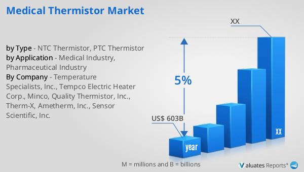
Based on our research, the global market for medical devices is projected to reach approximately $603 billion in 2023, with an anticipated growth rate of 5% annually over the next six years. This growth is indicative of the increasing demand for advanced medical technologies and the continuous innovation within the healthcare sector. The expansion of the medical device market is driven by several factors, including the rising prevalence of chronic diseases, an aging global population, and the growing emphasis on improving healthcare infrastructure worldwide. As healthcare systems strive to enhance patient care and outcomes, the demand for sophisticated medical devices, including thermistors, is expected to rise. Thermistors, with their critical role in temperature monitoring and control, are integral to the development and functionality of many medical devices. Their ability to provide precise and reliable temperature measurements ensures the safety and effectiveness of medical treatments, contributing to the overall growth of the medical device market. As the market continues to expand, manufacturers are focusing on developing innovative thermistor technologies to meet the evolving needs of the healthcare industry, ultimately driving further advancements in medical technology and improving patient care globally.


Report Metric Details
Report Name Medical Thermistor Market
Accounted market size in year US$ 603 billion
CAGR 5%
Base Year year
by Type
  • NTC Thermistor
  • PTC Thermistor
by Application
  • Medical Industry
  • Pharmaceutical Industry
Production by Region
  • North America
  • Europe
  • China
  • Japan
  • South Korea
Consumption by Region
  • North America (United States, Canada)
  • Europe (Germany, France, UK, Italy, Russia)
  • Asia-Pacific (China, Japan, South Korea, Taiwan)
  • Southeast Asia (India)
  • Latin America (Mexico, Brazil)
By Company Temperature Specialists, Inc., Tempco Electric Heater Corp., Minco, Quality Thermistor, Inc., Therm-X, Ametherm, Inc., Sensor Scientific, Inc.
Forecast units USD million in value
Report coverage Revenue and volume forecast, company share, competitive landscape, growth factors and trends

Global Copper Polishing Slurry Market Research Report 2025

What is Global Copper Polishing Slurry Market?

The Global Copper Polishing Slurry Market is a specialized segment within the broader semiconductor industry, focusing on the materials used in the chemical mechanical planarization (CMP) process. CMP is a critical step in semiconductor manufacturing, where a slurry is used to smooth and flatten the surface of semiconductor wafers, particularly those made of copper. This process is essential for creating the intricate patterns required for modern electronic devices. The slurry typically consists of abrasive particles suspended in a chemical solution, which helps to remove excess material and achieve the desired surface finish. The demand for copper polishing slurry is driven by the increasing complexity of semiconductor devices and the need for higher performance and miniaturization. As technology advances, the requirements for precision and efficiency in the CMP process become more stringent, leading to innovations in slurry formulations. The market is characterized by a focus on developing slurries that offer improved removal rates, selectivity, and defectivity, while also being environmentally friendly. This market is poised for growth as the semiconductor industry continues to expand, driven by the proliferation of electronic devices and the ongoing development of new technologies.

Copper Polishing Slurry Market

Colloidal Silica Based Slurry, Alumina Based Slurry in the Global Copper Polishing Slurry Market:

Colloidal silica-based slurry and alumina-based slurry are two prominent types of slurries used in the Global Copper Polishing Slurry Market, each with distinct characteristics and applications. Colloidal silica-based slurry is known for its fine particle size and uniform distribution, which makes it ideal for achieving a high-quality surface finish with minimal defects. The silica particles are suspended in a chemical solution that facilitates the removal of excess copper material during the CMP process. This type of slurry is particularly effective in applications where a smooth and defect-free surface is critical, such as in the production of advanced semiconductor devices. The chemical composition of colloidal silica-based slurry can be tailored to enhance its performance, allowing for precise control over the polishing process. On the other hand, alumina-based slurry is characterized by its harder abrasive particles, which provide a higher removal rate compared to colloidal silica-based slurry. This makes it suitable for applications where rapid material removal is necessary, such as in the initial stages of the CMP process. Alumina-based slurry is often used in conjunction with other types of slurries to achieve the desired balance between removal rate and surface finish. The choice between colloidal silica-based and alumina-based slurry depends on the specific requirements of the application, including the type of semiconductor device being manufactured and the desired surface characteristics. Both types of slurries play a crucial role in the CMP process, contributing to the overall efficiency and effectiveness of semiconductor manufacturing. As the demand for more advanced and miniaturized electronic devices continues to grow, the development of new and improved slurry formulations will be essential to meet the evolving needs of the industry.

Logic Chips, Memory Chips, Advanced Packaging in the Global Copper Polishing Slurry Market:

The Global Copper Polishing Slurry Market plays a vital role in the production of various semiconductor components, including logic chips, memory chips, and advanced packaging. Logic chips, which are used to perform the processing functions in electronic devices, require a high degree of precision and accuracy during manufacturing. The CMP process, facilitated by copper polishing slurry, is essential for creating the intricate patterns and structures needed for these chips to function effectively. The slurry helps to achieve the necessary surface planarity and smoothness, ensuring that the logic chips can operate at high speeds and with minimal power consumption. Memory chips, which are used to store data in electronic devices, also benefit from the use of copper polishing slurry. The CMP process helps to create the fine structures required for high-density memory storage, allowing for greater data capacity and faster access times. The use of copper polishing slurry in the production of memory chips is critical for meeting the increasing demand for more powerful and efficient storage solutions. Advanced packaging, which involves the integration of multiple semiconductor components into a single package, also relies on the CMP process and copper polishing slurry. This process is essential for ensuring the proper alignment and connection of the various components, which is crucial for the performance and reliability of the final product. The use of copper polishing slurry in advanced packaging helps to achieve the necessary surface finish and planarity, enabling the production of more compact and efficient electronic devices. As the semiconductor industry continues to evolve, the role of copper polishing slurry in the production of logic chips, memory chips, and advanced packaging will remain critical, driving further innovation and development in this market.

Global Copper Polishing Slurry Market Outlook:

In 2024, the global market for Copper Polishing Slurry was valued at approximately $540 million, and it is anticipated to grow to a revised size of $798 million by 2031, reflecting a compound annual growth rate (CAGR) of 5.8% over the forecast period. This growth is indicative of the increasing demand for advanced semiconductor devices and the critical role that copper polishing slurry plays in their production. The broader semiconductor market was estimated at $526.8 billion in 2023 and is projected to reach $780.7 billion by 2030. This expansion underscores the rapid advancements in technology and the growing need for more sophisticated electronic components. Additionally, the global semiconductor manufacturing wafer fabrication market is expected to grow from $251.7 billion in 2023 to $506.5 billion by 2030, with a remarkable CAGR of 40.49% during the forecast period. This significant growth highlights the importance of copper polishing slurry in the semiconductor manufacturing process, as it is essential for achieving the precision and quality required for modern electronic devices. The continued development and innovation in slurry formulations will be crucial for supporting the evolving needs of the semiconductor industry and maintaining the momentum of market growth.


Report Metric Details
Report Name Copper Polishing Slurry Market
Accounted market size in year US$ 540 million
Forecasted market size in 2031 US$ 798 million
CAGR 5.8%
Base Year year
Forecasted years 2025 - 2031
by Type
  • Colloidal Silica Based Slurry
  • Alumina Based Slurry
by Application
  • Logic Chips
  • Memory Chips
  • Advanced Packaging
Production by Region
  • North America
  • Europe
  • China
  • Japan
  • South Korea
Consumption by Region
  • North America (United States, Canada)
  • Europe (Germany, France, UK, Italy, Russia)
  • Asia-Pacific (China, Japan, South Korea, Taiwan)
  • Southeast Asia (India)
  • Latin America (Mexico, Brazil)
By Company Fujifilm, Resonac, FUJIMI INCORPORATED, DuPont, Merck (Versum Materials), Anjimirco Shanghai, Soulbrain, Saint-Gobain, Vibrantz (Ferro), TOPPAN INFOMEDIA CO., LTD, Samsung SDI
Forecast units USD million in value
Report coverage Revenue and volume forecast, company share, competitive landscape, growth factors and trends

Global CMP Tungsten Polishing Fluid Market Research Report 2025

What is Global CMP Tungsten Polishing Fluid Market?

The Global CMP Tungsten Polishing Fluid Market is a specialized segment within the semiconductor industry, focusing on the chemical mechanical planarization (CMP) process. CMP is a critical step in semiconductor manufacturing, used to smooth and flatten the surface of semiconductor wafers. Tungsten polishing fluids are specifically designed for the CMP of tungsten, a metal commonly used in semiconductor devices for its excellent electrical conductivity and thermal properties. These fluids are formulated with a combination of chemicals and abrasives that work together to remove excess material and achieve the desired surface finish. The demand for CMP tungsten polishing fluids is driven by the increasing complexity of semiconductor devices, which require precise and uniform surfaces to function effectively. As technology advances, the need for high-performance polishing fluids that can deliver consistent results becomes even more crucial. The market is characterized by continuous innovation, with manufacturers striving to develop formulations that offer improved performance, reduced environmental impact, and cost-effectiveness. The growth of the semiconductor industry, particularly in regions like Asia-Pacific, further fuels the demand for these specialized fluids, making the Global CMP Tungsten Polishing Fluid Market a dynamic and evolving sector.

CMP Tungsten Polishing Fluid Market

in the Global CMP Tungsten Polishing Fluid Market:

The Global CMP Tungsten Polishing Fluid Market caters to a diverse range of customers, each with specific requirements based on their applications and technological needs. These fluids are primarily used by semiconductor manufacturers, who rely on them to achieve the precise surface planarization required for advanced semiconductor devices. The types of CMP tungsten polishing fluids vary based on their chemical composition, abrasive content, and intended application. Some fluids are designed for high removal rates, making them suitable for applications where rapid material removal is necessary. These are often used in the initial stages of the CMP process, where large amounts of material need to be removed quickly. Other fluids are formulated for low defectivity, focusing on minimizing surface defects and achieving a high-quality finish. These are typically used in the final stages of polishing, where precision and surface quality are paramount. Additionally, there are fluids specifically designed for use with certain types of equipment or processes, such as those compatible with specific polishing pads or slurry delivery systems. The choice of fluid depends on various factors, including the type of semiconductor device being manufactured, the specific requirements of the CMP process, and the desired balance between performance and cost. For instance, manufacturers of DRAM and 3D NAND devices may prioritize high removal rates to meet the demands of high-volume production, while those producing logic ICs might focus on achieving the highest possible surface quality to ensure optimal device performance. The market also sees a demand for environmentally friendly formulations, as manufacturers seek to reduce the environmental impact of their processes. This has led to the development of polishing fluids that use less hazardous chemicals and generate less waste, aligning with broader industry trends towards sustainability. Furthermore, the market is influenced by regional variations, with different regions exhibiting distinct preferences and requirements based on their local semiconductor industries. In Asia-Pacific, for example, the rapid growth of the semiconductor sector drives a high demand for advanced CMP solutions, while in North America and Europe, there may be a greater emphasis on innovation and the development of next-generation technologies. Overall, the Global CMP Tungsten Polishing Fluid Market is characterized by a wide range of products tailored to meet the diverse needs of its customers, reflecting the complexity and dynamism of the semiconductor industry.

DRAM, 3D NAND, Logic IC, Others in the Global CMP Tungsten Polishing Fluid Market:

The usage of Global CMP Tungsten Polishing Fluid Market extends across various areas of semiconductor manufacturing, including DRAM, 3D NAND, Logic IC, and others. In the production of DRAM (Dynamic Random-Access Memory), CMP tungsten polishing fluids play a crucial role in ensuring the smooth and uniform surfaces required for efficient memory cell operation. DRAM devices are characterized by their high density and need for rapid data access, which necessitates precise manufacturing processes. The polishing fluids used in DRAM production are typically formulated to achieve high removal rates and low defectivity, balancing speed and quality to meet the demands of high-volume manufacturing. In the case of 3D NAND, a type of non-volatile memory that stacks memory cells vertically to increase storage capacity, CMP tungsten polishing fluids are essential for creating the intricate multi-layer structures. The fluids used in 3D NAND production must be capable of handling the complex geometries and tight tolerances associated with these advanced devices. They are often designed to provide excellent planarization and surface finish, ensuring the reliability and performance of the final product. For Logic ICs (Integrated Circuits), which are used in a wide range of applications from consumer electronics to industrial systems, CMP tungsten polishing fluids are critical for achieving the high levels of precision and surface quality required for optimal device performance. Logic ICs often involve complex circuit designs and require polishing fluids that can deliver consistent results across different layers and materials. The fluids used in this area are typically formulated to minimize defects and ensure uniformity, supporting the production of high-performance and reliable devices. Beyond these specific applications, CMP tungsten polishing fluids are also used in other areas of semiconductor manufacturing, such as the production of microprocessors, sensors, and other advanced electronic components. In these applications, the choice of polishing fluid is influenced by factors such as the specific materials being processed, the desired surface characteristics, and the overall manufacturing goals. As the semiconductor industry continues to evolve, the demand for high-performance CMP tungsten polishing fluids is expected to grow, driven by the increasing complexity and sophistication of semiconductor devices.

Global CMP Tungsten Polishing Fluid Market Outlook:

In 2024, the global market for CMP Tungsten Polishing Fluid was valued at approximately $586 million. By 2031, it is anticipated to expand to a revised size of $975 million, reflecting a compound annual growth rate (CAGR) of 7.7% over the forecast period. Meanwhile, the broader semiconductor market was estimated at $526.8 billion in 2023 and is projected to reach $780.7 billion by 2030. Our research indicates that the global semiconductor manufacturing wafer fabrication market is expected to grow significantly, from $251.7 billion in 2023 to $506.5 billion by 2030, with a remarkable CAGR of 40.49% during this period. These projections underscore the robust growth and dynamic nature of the semiconductor industry, driven by technological advancements and increasing demand for electronic devices. The CMP Tungsten Polishing Fluid Market, as a critical component of semiconductor manufacturing, is poised to benefit from these trends, with manufacturers focusing on innovation and efficiency to meet the evolving needs of the industry. The growth in wafer fabrication, in particular, highlights the increasing complexity and sophistication of semiconductor devices, necessitating advanced CMP solutions to ensure high-quality production. As the market continues to expand, companies are likely to invest in research and development to enhance the performance and sustainability of their polishing fluids, aligning with broader industry trends towards innovation and environmental responsibility.


Report Metric Details
Report Name CMP Tungsten Polishing Fluid Market
Accounted market size in year US$ 586 million
Forecasted market size in 2031 US$ 975 million
CAGR 7.7%
Base Year year
Forecasted years 2025 - 2031
by Application
  • DRAM
  • 3D NAND
  • Logic IC
  • Others
Production by Region
  • North America
  • South Korea
  • China
  • Japan
  • China Taiwan
Consumption by Region
  • North America (United States, Canada)
  • Europe (Germany, France, UK, Italy, Russia)
  • Asia-Pacific (China, Japan, South Korea, Taiwan)
  • Southeast Asia (India)
  • Latin America (Mexico, Brazil)
By Company Fujifilm, DuPont, Merck KGaA (Versum Materials), KC Tech, Dongjin Semichem, Anjimirco Shanghai, Samsung SDI, JSR Corporation, Vibrantz (Ferro), Hubei Dinglong, by Abrasive Type, Fumed Silica, High Purity Colloidal Silica
Forecast units USD million in value
Report coverage Revenue and volume forecast, company share, competitive landscape, growth factors and trends

Global Semiconductor Silicon Polishing Wafer Market Research Report 2025

What is Global Semiconductor Silicon Polishing Wafer Market?

The Global Semiconductor Silicon Polishing Wafer Market is a crucial segment within the semiconductor industry, focusing on the production and refinement of silicon wafers. These wafers are thin slices of semiconductor material, primarily silicon, which serve as the foundational substrate for fabricating integrated circuits and other microdevices. The market encompasses various processes and technologies aimed at enhancing the quality and performance of these wafers, including polishing, which is essential for achieving the smooth, defect-free surfaces required for advanced electronic applications. As the demand for smaller, more powerful, and energy-efficient electronic devices continues to grow, the need for high-quality silicon wafers has become increasingly critical. This market is driven by technological advancements, increased production capacities, and the expanding applications of semiconductors in various industries, including consumer electronics, automotive, telecommunications, and artificial intelligence. The global semiconductor silicon polishing wafer market is characterized by intense competition among key players, continuous innovation, and a focus on sustainability and cost-effectiveness. As a result, companies are investing heavily in research and development to improve wafer quality and production efficiency, ensuring they meet the evolving needs of the semiconductor industry.

Semiconductor Silicon Polishing Wafer Market

Less than 150 mm, 200 mm, 300 mm, Other(450 mm) in the Global Semiconductor Silicon Polishing Wafer Market:

In the Global Semiconductor Silicon Polishing Wafer Market, wafers are categorized based on their diameter, which significantly impacts their application and production processes. Wafers less than 150 mm in diameter are typically used in niche applications and older semiconductor technologies. These smaller wafers are often employed in the production of discrete components and specialized devices where the demand for high-volume production is lower. Despite their limited use in cutting-edge technologies, they remain essential for certain legacy systems and specific industrial applications. Moving to 200 mm wafers, these have been a staple in the semiconductor industry for many years. They are widely used in the production of a variety of semiconductor devices, including microcontrollers, sensors, and analog devices. The 200 mm wafers strike a balance between cost and performance, making them suitable for a broad range of applications, particularly in consumer electronics and automotive industries. As the industry progresses, the demand for 200 mm wafers continues to be strong, driven by the need for more sophisticated electronic components in everyday devices. The 300 mm wafers represent the current standard for high-volume semiconductor manufacturing. These larger wafers allow for more chips to be produced per wafer, significantly reducing the cost per chip and increasing production efficiency. The transition to 300 mm wafers has been driven by the need for higher performance and lower costs in the production of advanced semiconductor devices, such as microprocessors and memory chips. The use of 300 mm wafers is prevalent in the production of cutting-edge technologies, including those used in smartphones, data centers, and high-performance computing. Finally, the category of "Other" includes wafers with diameters of 450 mm and beyond. While still in the developmental and experimental stages, these larger wafers hold the potential to revolutionize the semiconductor industry by further reducing costs and increasing production efficiency. However, the transition to 450 mm wafers presents significant technical and economic challenges, requiring substantial investment in new manufacturing equipment and processes. Despite these challenges, the potential benefits of 450 mm wafers continue to drive research and development efforts, as the industry seeks to meet the growing demand for more powerful and cost-effective semiconductor solutions.

Electronic communication, Consumer Electronics, Artificial Intelligence, Other in the Global Semiconductor Silicon Polishing Wafer Market:

The Global Semiconductor Silicon Polishing Wafer Market plays a pivotal role in various sectors, including electronic communication, consumer electronics, artificial intelligence, and other emerging fields. In electronic communication, silicon wafers are fundamental in the production of integrated circuits used in communication devices such as smartphones, tablets, and networking equipment. The demand for faster and more reliable communication technologies drives the need for high-quality wafers that can support advanced functionalities and higher data transfer rates. In consumer electronics, silicon wafers are essential for manufacturing a wide range of devices, from televisions and gaming consoles to wearable technology and smart home devices. The continuous evolution of consumer electronics, with a focus on miniaturization and enhanced performance, necessitates the use of superior silicon wafers that can accommodate complex circuitry and high-density integration. In the realm of artificial intelligence, silicon wafers are crucial for developing powerful processors and specialized chips that enable machine learning and data processing capabilities. As AI technologies become more prevalent across industries, the demand for advanced semiconductor solutions, including high-performance silicon wafers, is expected to grow. Beyond these areas, the Global Semiconductor Silicon Polishing Wafer Market also supports other sectors such as automotive, healthcare, and industrial automation. In the automotive industry, silicon wafers are used in the production of sensors, microcontrollers, and other electronic components that are integral to modern vehicles' safety, efficiency, and connectivity features. In healthcare, semiconductor devices play a vital role in medical imaging, diagnostics, and wearable health monitoring systems, all of which rely on high-quality silicon wafers for their operation. Industrial automation, too, benefits from the advancements in semiconductor technology, with silicon wafers being used in the development of control systems, robotics, and other automated solutions. As these industries continue to evolve and expand, the Global Semiconductor Silicon Polishing Wafer Market is poised to play an increasingly important role in supporting technological innovation and meeting the growing demand for advanced electronic solutions.

Global Semiconductor Silicon Polishing Wafer Market Outlook:

The outlook for the Global Semiconductor Silicon Polishing Wafer Market is promising, with significant growth anticipated over the coming years. In 2022, the global semiconductor market was valued at approximately $579 billion, and it is projected to reach $790 billion by 2029, reflecting a compound annual growth rate (CAGR) of 6% during the forecast period. This growth is driven by several factors, including the increasing demand for semiconductors in various applications, such as consumer electronics, automotive, telecommunications, and artificial intelligence. As technology continues to advance, the need for more powerful, efficient, and cost-effective semiconductor solutions is expected to rise, further fueling the market's expansion. Additionally, the ongoing development of new technologies, such as 5G, the Internet of Things (IoT), and advanced driver-assistance systems (ADAS), is expected to create new opportunities for the semiconductor industry, driving demand for high-quality silicon wafers. As a result, companies within the Global Semiconductor Silicon Polishing Wafer Market are likely to continue investing in research and development to enhance wafer quality, production efficiency, and sustainability, ensuring they remain competitive in this rapidly evolving industry.


Report Metric Details
Report Name Semiconductor Silicon Polishing Wafer Market
Accounted market size in year US$ 579 billion
Forecasted market size in 2029 US$ 790 billion
CAGR 6%
Base Year year
Forecasted years 2025 - 2029
by Type
  • Less than 150 mm
  • 200 mm
  • 300 mm
  • Other(450 mm)
by Application
  • Electronic communication
  • Consumer Electronics
  • Artificial Intelligence
  • Other
Production by Region
  • North America
  • Europe
  • China
  • Japan
  • South Korea
Consumption by Region
  • North America (United States, Canada)
  • Europe (Germany, France, UK, Italy, Russia)
  • Asia-Pacific (China, Japan, South Korea, Taiwan)
  • Southeast Asia (India)
  • Latin America (Mexico, Brazil)
By Company Shin-Etsu Chemical, Sumco, Global Wafers, Siltronic, SK siltron, Waferworks, Ferrotec, AST, Gritek, Guosheng, QL Electronics, MCL, National Silicon Industry Group, GRINM Semiconductor Materials Co., Ltd., ThinkonSemi, Tianjin Zhonghuan Semiconducto, Hangzhou Leon Dongxin Microelectronics, Wafer Technology, Hangzhou Zhongxin Wafer Semiconductor, Tianjin Zhongjing Semiconductor Materials Co., Ltd., Suzhou New Micron Nano Technology, ESWIN
Forecast units USD million in value
Report coverage Revenue and volume forecast, company share, competitive landscape, growth factors and trends

Global Ferrite Multilayer Inductor Market Research Report 2025

What is Global Ferrite Multilayer Inductor Market?

The Global Ferrite Multilayer Inductor Market is a crucial segment within the electronics industry, characterized by its role in managing electrical currents and signals in various devices. Ferrite multilayer inductors are passive electronic components that store energy in a magnetic field when electric current flows through them. They are constructed using ferrite, a type of ceramic material that is highly effective in reducing electromagnetic interference. These inductors are essential in ensuring the smooth operation of electronic circuits by filtering noise and stabilizing voltage. The market for these components is driven by the increasing demand for miniaturized electronic devices, which require compact and efficient inductors. As technology advances, the need for high-performance inductors in applications such as smartphones, laptops, and other consumer electronics continues to grow. Additionally, the automotive and telecommunications sectors are significant contributors to the market's expansion, as they increasingly incorporate advanced electronic systems that rely on these inductors. The global market is also influenced by the rising trend of the Internet of Things (IoT), which necessitates the integration of numerous electronic components into everyday objects, further boosting the demand for ferrite multilayer inductors.

Ferrite Multilayer Inductor Market

Chip Type, Wire Wound Type, Other in the Global Ferrite Multilayer Inductor Market:

In the Global Ferrite Multilayer Inductor Market, different types of inductors cater to various applications and requirements. Chip type inductors are among the most common, known for their compact size and efficiency. These inductors are typically used in high-frequency applications, such as RF circuits and power supplies, due to their ability to handle high currents and frequencies. Their small size makes them ideal for use in compact electronic devices, where space is at a premium. Chip type inductors are often found in smartphones, tablets, and other portable electronics, where they help manage power distribution and signal integrity. Wire wound type inductors, on the other hand, are known for their high inductance values and current handling capabilities. These inductors are constructed by winding a wire around a core, usually made of ferrite or another magnetic material. Wire wound inductors are commonly used in power applications, such as power converters and inverters, where they help regulate voltage and current. They are also used in audio equipment, where they contribute to sound quality by filtering out unwanted noise. Other types of inductors in the market include multilayer inductors, which are constructed by stacking multiple layers of conductive material and insulating layers. These inductors offer a balance between size and performance, making them suitable for a wide range of applications. They are often used in telecommunications equipment, where they help manage signal integrity and reduce electromagnetic interference. The choice of inductor type depends on the specific requirements of the application, including factors such as size, frequency, and current handling capabilities. As technology continues to evolve, the demand for specialized inductors that can meet the needs of emerging applications is expected to grow, driving further innovation in the Global Ferrite Multilayer Inductor Market.

Consumer Electronics, Automotive, IoT, Medical Equipment, Defense & Aerospace, Other in the Global Ferrite Multilayer Inductor Market:

The usage of Global Ferrite Multilayer Inductor Market spans across various industries, each with its unique requirements and applications. In the consumer electronics sector, these inductors are integral to the functioning of devices such as smartphones, laptops, and tablets. They help manage power distribution, filter noise, and ensure signal integrity, contributing to the overall performance and reliability of these devices. As consumer electronics continue to evolve, with increasing demands for smaller, more efficient components, the role of ferrite multilayer inductors becomes even more critical. In the automotive industry, the adoption of advanced electronic systems has led to a growing demand for these inductors. They are used in various applications, including engine control units, infotainment systems, and advanced driver-assistance systems (ADAS), where they help manage power and signal integrity. The rise of electric and hybrid vehicles further amplifies the need for efficient inductors, as these vehicles rely heavily on electronic components for their operation. The Internet of Things (IoT) is another area where ferrite multilayer inductors play a vital role. As more devices become interconnected, the need for efficient power management and signal integrity becomes paramount. Inductors are used in IoT devices to filter noise and ensure reliable communication between devices, contributing to the seamless operation of IoT networks. In the medical equipment industry, ferrite multilayer inductors are used in various devices, including imaging equipment, patient monitoring systems, and diagnostic tools. They help ensure the accuracy and reliability of these devices by managing power distribution and filtering out unwanted noise. The defense and aerospace sectors also rely on these inductors for their advanced electronic systems. They are used in communication systems, radar equipment, and navigation systems, where they help manage power and ensure signal integrity. The demand for reliable and efficient inductors in these sectors is driven by the need for high-performance electronic systems that can operate in challenging environments. Other industries, such as telecommunications and industrial automation, also benefit from the use of ferrite multilayer inductors, as they help manage power and signal integrity in various applications. As technology continues to advance, the demand for these inductors is expected to grow, driven by the need for efficient and reliable electronic components across various industries.

Global Ferrite Multilayer Inductor Market Outlook:

The global market for Ferrite Multilayer Inductor was valued at $715 million in 2024, and it is anticipated to expand significantly, reaching an estimated $1,314 million by 2031. This growth trajectory represents a compound annual growth rate (CAGR) of 9.2% over the forecast period. This substantial increase underscores the rising demand for ferrite multilayer inductors across various industries, driven by technological advancements and the increasing need for efficient electronic components. The market's expansion is fueled by the growing adoption of miniaturized electronic devices, which require compact and high-performance inductors to ensure optimal functionality. Additionally, the automotive and telecommunications sectors are significant contributors to this growth, as they increasingly incorporate advanced electronic systems that rely on these inductors. The rise of the Internet of Things (IoT) further amplifies the demand for ferrite multilayer inductors, as more devices become interconnected, necessitating efficient power management and signal integrity. As industries continue to evolve and embrace new technologies, the global market for ferrite multilayer inductors is poised for sustained growth, driven by the need for reliable and efficient electronic components.


Report Metric Details
Report Name Ferrite Multilayer Inductor Market
Accounted market size in year US$ 715 million
Forecasted market size in 2031 US$ 1314 million
CAGR 9.2%
Base Year year
Forecasted years 2025 - 2031
by Type
  • Chip Type
  • Wire Wound Type
  • Other
by Application
  • Consumer Electronics
  • Automotive
  • IoT
  • Medical Equipment
  • Defense & Aerospace
  • Other
Production by Region
  • North America
  • Europe
  • China
  • Japan
  • South Korea
  • China Taiwan
Consumption by Region
  • North America (United States, Canada)
  • Europe (Germany, France, UK, Italy, Russia)
  • Asia-Pacific (China, Japan, South Korea, Taiwan)
  • Southeast Asia (India)
  • Latin America (Mexico, Brazil)
By Company TDK, Shenzhen Zhenhua Fu Electronics, Chilisin Electronics (YAGEO), Vishay, Fenghua Advanced Technology, KOHER (Shanghai) Electronic, Laird Technologies, Microgate Technology, INPAQ Technology, Darfon Electronics
Forecast units USD million in value
Report coverage Revenue and volume forecast, company share, competitive landscape, growth factors and trends

Global Positive Photoresist for ICs Market Research Report 2025

What is Global Positive Photoresist for ICs Market?

The Global Positive Photoresist for ICs Market refers to the worldwide industry focused on the production and application of positive photoresist materials used in the manufacturing of integrated circuits (ICs). Positive photoresists are light-sensitive materials that become soluble when exposed to light, allowing for precise patterning on semiconductor wafers. This process is crucial in the fabrication of ICs, which are the building blocks of modern electronic devices. The market encompasses various types of photoresists, each tailored for specific wavelengths of light used in photolithography, a key step in semiconductor manufacturing. The demand for positive photoresists is driven by the growing need for advanced electronic devices, including smartphones, computers, and other consumer electronics, as well as the expansion of industries such as automotive, telecommunications, and aerospace. As technology advances, the market continues to evolve, with innovations aimed at improving the resolution and efficiency of photoresist materials to meet the demands of next-generation semiconductor devices.

Positive Photoresist for ICs Market

G Line Photoresist, I Line Photoresist, KrF Photoresist, ArF Photoresist, EUV Photoresist in the Global Positive Photoresist for ICs Market:

G Line Photoresist, I Line Photoresist, KrF Photoresist, ArF Photoresist, and EUV Photoresist are different types of positive photoresists used in the Global Positive Photoresist for ICs Market, each designed for specific photolithography processes. G Line Photoresist is sensitive to the G-line of mercury vapor lamps, which emits light at a wavelength of 436 nanometers. It is one of the older technologies but remains in use for certain applications due to its cost-effectiveness and adequate performance for less demanding processes. I Line Photoresist, on the other hand, is sensitive to the I-line, with a wavelength of 365 nanometers. It offers better resolution than G Line Photoresist and is widely used in the production of microelectronics where finer patterning is required. KrF Photoresist is designed for use with krypton fluoride (KrF) excimer lasers, which emit light at 248 nanometers. This type of photoresist allows for even finer patterning, making it suitable for more advanced semiconductor manufacturing processes. ArF Photoresist is used with argon fluoride (ArF) excimer lasers, which have a wavelength of 193 nanometers. This technology enables the production of extremely small and precise features on semiconductor wafers, supporting the development of high-performance ICs. Finally, EUV Photoresist is designed for extreme ultraviolet (EUV) lithography, which operates at a wavelength of 13.5 nanometers. EUV Photoresist represents the cutting edge of photolithography technology, allowing for the creation of incredibly small features necessary for the latest generation of semiconductor devices. Each type of photoresist plays a crucial role in the semiconductor manufacturing process, with the choice of photoresist depending on the specific requirements of the ICs being produced, such as feature size, complexity, and production volume. As the demand for more powerful and efficient electronic devices continues to grow, the development and refinement of these photoresist technologies remain a key focus for the industry.

Consumer Electronics, Automotive, Industrial Electronics, Aerospace and Defence, Telecommunications, Others in the Global Positive Photoresist for ICs Market:

The usage of Global Positive Photoresist for ICs Market spans several key areas, including consumer electronics, automotive, industrial electronics, aerospace and defense, telecommunications, and others. In consumer electronics, positive photoresists are essential for the production of integrated circuits used in devices such as smartphones, tablets, laptops, and wearable technology. The demand for smaller, faster, and more energy-efficient devices drives the need for advanced photoresist materials that can support the production of high-density ICs with intricate patterns. In the automotive sector, the increasing integration of electronic components in vehicles, such as advanced driver-assistance systems (ADAS), infotainment systems, and electric vehicle powertrains, relies heavily on the use of ICs manufactured with positive photoresists. These materials enable the production of reliable and high-performance semiconductor components that meet the stringent requirements of the automotive industry. Industrial electronics also benefit from the use of positive photoresists, as they are used in the manufacturing of ICs for automation systems, sensors, and control units that are critical for industrial applications. In the aerospace and defense sectors, positive photoresists are used in the production of specialized ICs for communication systems, navigation, and surveillance equipment, where precision and reliability are paramount. Telecommunications is another area where positive photoresists play a vital role, as they are used in the production of ICs for network infrastructure, mobile devices, and communication satellites. The demand for faster and more reliable communication networks drives the need for advanced photoresist materials that can support the production of high-performance semiconductor components. Other areas where positive photoresists are used include medical devices, where they are used in the production of ICs for diagnostic equipment and implantable devices, and renewable energy, where they are used in the manufacturing of ICs for solar panels and wind turbines. Overall, the Global Positive Photoresist for ICs Market is integral to the advancement of technology across various industries, enabling the production of sophisticated electronic components that power modern devices and systems.

Global Positive Photoresist for ICs Market Outlook:

The global market for Positive Photoresist for ICs was valued at $20,200 million in 2024 and is anticipated to expand to a revised size of $32,530 million by 2031, reflecting a compound annual growth rate (CAGR) of 7.1% over the forecast period. This growth trajectory underscores the increasing demand for positive photoresist materials in the semiconductor industry, driven by the rapid advancement of technology and the proliferation of electronic devices across various sectors. The market's expansion is fueled by the continuous innovation in photoresist technologies, which are essential for the production of smaller, faster, and more efficient integrated circuits. As industries such as consumer electronics, automotive, telecommunications, and aerospace continue to evolve, the need for high-performance semiconductor components becomes more pronounced, further propelling the demand for positive photoresists. The market's growth is also supported by the increasing adoption of advanced photolithography techniques, such as EUV lithography, which require specialized photoresist materials to achieve the desired level of precision and resolution. As a result, the Global Positive Photoresist for ICs Market is poised for significant growth, driven by the ongoing advancements in semiconductor manufacturing and the ever-increasing demand for cutting-edge electronic devices.


Report Metric Details
Report Name Positive Photoresist for ICs Market
Accounted market size in year US$ 20200 million
Forecasted market size in 2031 US$ 32530 million
CAGR 7.1%
Base Year year
Forecasted years 2025 - 2031
by Type
  • G Line Photoresist
  • I Line Photoresist
  • KrF Photoresist
  • ArF Photoresist
  • EUV Photoresist
by Application
  • Consumer Electronics
  • Automotive
  • Industrial Electronics
  • Aerospace and Defence
  • Telecommunications
  • Others
Production by Region
  • North America
  • Europe
  • China
  • Japan
  • South Korea
  • China Taiwan
Consumption by Region
  • North America (United States, Canada)
  • Europe (Germany, France, UK, Italy, Russia)
  • Asia-Pacific (China, Japan, South Korea, Taiwan)
  • Southeast Asia (India)
  • Latin America (Mexico, Brazil)
By Company TOKYO OHKA KOGYO CO., LTD. (TOK), JSR, Shin-Etsu Chemical, DuPont, Fujifilm, Sumitomo Chemical, Dongjin Semichem, Merck KGaA (AZ), Allresist GmbH, Futurrex, KemLab™ Inc, YCCHEM Co., Ltd, SK Materials Performance (SKMP), Everlight Chemical, Red Avenue, Crystal Clear Electronic Material, Xuzhou B & C Chemical, Xiamen Hengkun New Material Technology, Jiangsu Aisen Semiconductor Material, Zhuhai Cornerstone Technologies, Shanghai Sinyang Semiconductor Materials, ShenZhen RongDa Photosensitive Science & Technology, SINEVA, Guoke Tianji, Jiangsu Nata Opto-electronic Material, PhiChem
Forecast units USD million in value
Report coverage Revenue and volume forecast, company share, competitive landscape, growth factors and trends

Global Semiconductor Tray Market Research Report 2025

What is Global Semiconductor Tray Market?

The Global Semiconductor Tray Market is an essential component of the semiconductor industry, providing specialized packaging solutions for the safe handling, storage, and transportation of semiconductor devices. These trays are designed to protect delicate semiconductor components from physical damage, contamination, and electrostatic discharge, ensuring their integrity and functionality throughout the supply chain. The market encompasses a variety of tray types, including waffle packs, matrix trays, and custom-designed solutions, each tailored to meet specific requirements of different semiconductor devices. As the demand for semiconductors continues to rise, driven by advancements in technology and the proliferation of electronic devices, the need for reliable and efficient semiconductor trays has become increasingly critical. Manufacturers in this market are constantly innovating to develop trays that offer enhanced protection, compatibility with automated handling systems, and compliance with industry standards. The global semiconductor tray market is characterized by a diverse range of materials, designs, and applications, reflecting the dynamic nature of the semiconductor industry and its evolving needs. As such, it plays a pivotal role in supporting the growth and development of the semiconductor sector, contributing to the seamless production and distribution of electronic components worldwide.

Semiconductor Tray Market

MPPE, PES, PS, ABS, Others in the Global Semiconductor Tray Market:

In the Global Semiconductor Tray Market, various materials are utilized to manufacture trays, each offering distinct properties and advantages. MPPE (Modified Polyphenylene Ether) is a popular choice due to its excellent thermal stability, dimensional stability, and resistance to chemicals. These properties make MPPE trays ideal for high-temperature applications and environments where chemical exposure is a concern. Additionally, MPPE trays are known for their lightweight nature, which facilitates easy handling and transportation. PES (Polyethersulfone) is another material commonly used in semiconductor trays. It is renowned for its high-temperature resistance, mechanical strength, and transparency. PES trays are particularly suitable for applications requiring visibility of the components within the tray, allowing for easy inspection and identification. The material's robustness ensures that it can withstand the rigors of automated handling systems without compromising the safety of the semiconductor devices. PS (Polystyrene) is a widely used material in the production of semiconductor trays due to its cost-effectiveness and ease of processing. PS trays offer good dimensional stability and are often used for general-purpose applications where high-temperature resistance is not a primary concern. However, they may not be suitable for environments with extreme temperature variations or exposure to harsh chemicals. ABS (Acrylonitrile Butadiene Styrene) is another material frequently employed in the semiconductor tray market. Known for its impact resistance and toughness, ABS trays provide excellent protection for semiconductor components during handling and transportation. The material's versatility allows for the production of trays with intricate designs and features, catering to the specific needs of different semiconductor devices. Additionally, ABS trays are compatible with various surface treatments, enhancing their performance in specific applications. Beyond these materials, the semiconductor tray market also includes trays made from other specialized materials, each offering unique benefits. For instance, some trays are manufactured using conductive or dissipative materials to prevent electrostatic discharge, a critical consideration in the semiconductor industry. Others may incorporate anti-static coatings or additives to enhance their protective capabilities. The choice of material for semiconductor trays is influenced by several factors, including the specific requirements of the semiconductor devices, the handling and transportation conditions, and the cost considerations. Manufacturers in the semiconductor tray market are continually exploring new materials and technologies to develop trays that meet the evolving demands of the semiconductor industry. This ongoing innovation ensures that semiconductor trays remain a vital component in the production and distribution of electronic components, providing the necessary protection and support for the advancement of technology.

Electronic Products, Electronic Parts, Others in the Global Semiconductor Tray Market:

The Global Semiconductor Tray Market plays a crucial role in the electronics industry, providing essential solutions for the handling and transportation of electronic products and parts. In the realm of electronic products, semiconductor trays are indispensable for the safe and efficient movement of finished goods, such as smartphones, tablets, and laptops, from manufacturing facilities to distribution centers and retail outlets. These trays ensure that electronic products are protected from physical damage, contamination, and electrostatic discharge during transit, preserving their quality and functionality. The use of semiconductor trays in the transportation of electronic products also facilitates efficient inventory management and logistics, enabling manufacturers and distributors to streamline their operations and reduce costs. In the context of electronic parts, semiconductor trays are vital for the handling and storage of individual components, such as integrated circuits, microchips, and sensors, throughout the production process. These trays provide a secure and organized means of transporting electronic parts between different stages of manufacturing, assembly, and testing, minimizing the risk of damage and contamination. The use of semiconductor trays in the handling of electronic parts also supports automated manufacturing processes, allowing for seamless integration with robotic handling systems and reducing the need for manual intervention. Beyond electronic products and parts, the Global Semiconductor Tray Market also serves other industries and applications where the safe handling and transportation of sensitive components are critical. For instance, semiconductor trays are used in the automotive industry for the packaging and transportation of electronic control units and sensors, ensuring their protection and reliability. In the medical field, semiconductor trays are employed for the handling of medical devices and components, safeguarding their integrity and performance. The versatility and adaptability of semiconductor trays make them an essential component in various industries, supporting the efficient and reliable production and distribution of electronic and other sensitive components. As the demand for electronic products and parts continues to grow, driven by technological advancements and the increasing integration of electronics in everyday life, the Global Semiconductor Tray Market is poised to play an increasingly important role in supporting the electronics industry and its associated sectors.

Global Semiconductor Tray Market Outlook:

The global semiconductor market, valued at approximately $579 billion in 2022, is anticipated to reach around $790 billion by 2029, reflecting a compound annual growth rate (CAGR) of 6% over the forecast period. This growth trajectory underscores the expanding demand for semiconductors, driven by technological advancements and the increasing integration of electronic devices in various sectors. The semiconductor industry is pivotal in powering a wide array of applications, from consumer electronics and automotive systems to industrial machinery and telecommunications. As the world becomes more interconnected and reliant on digital technologies, the need for semiconductors is expected to rise, fueling the market's expansion. The projected growth of the semiconductor market also highlights the importance of innovation and investment in research and development to meet the evolving needs of consumers and industries. Companies operating in this space are likely to focus on enhancing the performance, efficiency, and sustainability of semiconductor products to maintain a competitive edge. Additionally, the semiconductor market's growth is likely to have a ripple effect on related industries, such as semiconductor manufacturing equipment, materials, and packaging solutions, further driving economic activity and technological progress. As the market continues to evolve, stakeholders across the semiconductor value chain will need to adapt to changing dynamics and capitalize on emerging opportunities to sustain growth and success.


Report Metric Details
Report Name Semiconductor Tray Market
Accounted market size in year US$ 579 billion
Forecasted market size in 2029 US$ 790 billion
CAGR 6%
Base Year year
Forecasted years 2025 - 2029
by Type
  • MPPE
  • PES
  • PS
  • ABS
  • Others
by Application
  • Electronic Products
  • Electronic Parts
  • Others
Production by Region
  • North America
  • Europe
  • China
  • Japan
  • South Korea
Consumption by Region
  • North America (United States, Canada)
  • Europe (Germany, France, UK, Italy, Russia)
  • Asia-Pacific (China, Japan, South Korea, Taiwan)
  • Southeast Asia (India)
  • Latin America (Mexico, Brazil)
By Company Daewon, Kostat, HWA SHU, SHINON, ePAK, Peak International, Mishima Kosan, ASE Group, ITW EBA, Entegris, RH Murphy Co, Shiima Electronics, Iwaki, MTI Corporation, KUNSHAN SUNRISE PLASTICS INDUSTRY, TOMOE Engineering, Hiner-pack, Shenzhen Prince New Materials, TIAN Shui HUA TIAN IC Packing MATERIALS
Forecast units USD million in value
Report coverage Revenue and volume forecast, company share, competitive landscape, growth factors and trends

Global Protective Clothing Synthetic Blood Penetration Tester Market Research Report 2025

What is Global Protective Clothing Synthetic Blood Penetration Tester Market? The Global Protective Clothing Synthetic Blood Penetration Te...