What is Global Epitaxial Wafer for Semiconductor Laser Market?
The Global Epitaxial Wafer for Semiconductor Laser Market is a specialized segment within the semiconductor industry that focuses on the production and utilization of epitaxial wafers specifically designed for semiconductor lasers. These wafers are crucial components in the manufacturing of semiconductor lasers, which are used in a variety of applications such as telecommunications, data storage, and medical devices. Epitaxial wafers are created through a process called epitaxy, where a crystalline layer is grown on a substrate wafer. This process allows for precise control over the material properties, which is essential for the performance and efficiency of semiconductor lasers. The market for these wafers is driven by the increasing demand for high-performance lasers in various industries, as well as advancements in technology that require more sophisticated and efficient laser components. As industries continue to innovate and expand, the need for high-quality epitaxial wafers is expected to grow, making this market a critical area of focus for semiconductor manufacturers and researchers alike.
2 Inch, 4 Inch, Others in the Global Epitaxial Wafer for Semiconductor Laser Market:
In the Global Epitaxial Wafer for Semiconductor Laser Market, wafers are typically categorized by their size, with common dimensions being 2-inch, 4-inch, and others. Each size category serves different needs and applications within the semiconductor laser industry. The 2-inch wafers are often used in applications where smaller, more compact laser components are required. These wafers are ideal for devices that need to be miniaturized without compromising on performance, such as in portable electronics or compact medical devices. The smaller size allows for greater precision in the manufacturing process, which can lead to improved performance and efficiency of the final laser product. On the other hand, 4-inch wafers are generally used in applications that require larger laser components or where higher power output is necessary. These wafers provide a larger surface area, which can be beneficial for producing more powerful lasers that are used in industrial applications, such as cutting and welding, or in telecommunications where high data transmission rates are needed. The larger size also allows for more efficient production processes, as multiple laser components can be fabricated on a single wafer, reducing costs and increasing throughput. In addition to the standard 2-inch and 4-inch sizes, there are other wafer sizes available in the market, which cater to specific niche applications or emerging technologies. These may include custom sizes that are tailored to the unique requirements of a particular application or industry. For example, in the field of photonics, where precise control over light is essential, custom-sized wafers may be used to optimize the performance of photonic devices. Similarly, in the development of next-generation communication technologies, such as 5G and beyond, specialized wafer sizes may be required to meet the demanding specifications of these advanced systems. The choice of wafer size is often determined by a combination of factors, including the intended application, the desired performance characteristics, and the cost considerations of the manufacturing process. As the semiconductor laser market continues to evolve, the demand for different wafer sizes is expected to change, driven by technological advancements and the emergence of new applications. Manufacturers in this market must remain agile and responsive to these changes, ensuring that they can provide the right wafer sizes to meet the needs of their customers. This requires a deep understanding of the market dynamics, as well as a commitment to innovation and quality in the production of epitaxial wafers.
DFB, EML and FP, VCSEL in the Global Epitaxial Wafer for Semiconductor Laser Market:
The Global Epitaxial Wafer for Semiconductor Laser Market finds its usage in several key areas, including Distributed Feedback (DFB) lasers, Electro-absorption Modulated Lasers (EML), Fabry-Pérot (FP) lasers, and Vertical-Cavity Surface-Emitting Lasers (VCSEL). Each of these laser types has specific applications and benefits from the unique properties of epitaxial wafers. DFB lasers are widely used in telecommunications for their ability to provide stable and narrow linewidths, which are essential for high-speed data transmission. The epitaxial wafers used in DFB lasers must have precise material properties to ensure the laser's performance and reliability. These wafers enable the creation of the grating structures that are integral to the DFB laser's operation, allowing for efficient and stable laser emission. EMLs, on the other hand, combine a laser with an electro-absorption modulator, making them ideal for high-speed data communication applications. The epitaxial wafers used in EMLs must support both the laser and modulator functions, requiring a high degree of precision in their fabrication. These wafers enable the integration of the laser and modulator on a single chip, reducing size and power consumption while increasing performance. FP lasers are simpler in design compared to DFB and EML lasers, making them cost-effective solutions for applications where high precision is not as critical. The epitaxial wafers used in FP lasers provide the necessary material properties for the laser's operation, ensuring consistent performance across a range of applications. These lasers are often used in consumer electronics and other applications where cost is a significant consideration. VCSELs are another important application area for epitaxial wafers, known for their efficiency and ability to emit light perpendicular to the surface of the wafer. This unique property makes VCSELs suitable for a variety of applications, including data communication, sensing, and 3D imaging. The epitaxial wafers used in VCSELs must support the vertical emission of light, requiring precise control over the wafer's material properties and structure. As the demand for high-performance lasers continues to grow across various industries, the role of epitaxial wafers in these applications becomes increasingly important. Manufacturers must ensure that their wafers meet the stringent requirements of each laser type, providing the necessary performance and reliability for their intended applications.
Global Epitaxial Wafer for Semiconductor Laser Market Outlook:
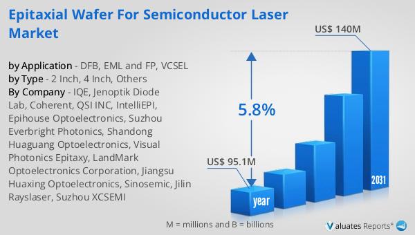
The global market for epitaxial wafers used in semiconductor lasers was valued at approximately $95.1 million in 2024. This market is anticipated to expand significantly, reaching an estimated value of $140 million by the year 2031. This growth represents a compound annual growth rate (CAGR) of 5.8% over the forecast period. This upward trend is indicative of the increasing demand for semiconductor lasers across various industries, driven by technological advancements and the need for more efficient and high-performance laser components. The growth in this market can be attributed to several factors, including the rising adoption of semiconductor lasers in telecommunications, data storage, and medical applications. As industries continue to innovate and develop new technologies, the demand for high-quality epitaxial wafers is expected to rise, supporting the growth of the market. Additionally, the increasing focus on energy efficiency and miniaturization in electronic devices is driving the need for more advanced semiconductor lasers, further boosting the demand for epitaxial wafers. Manufacturers in this market are likely to benefit from these trends, as they continue to develop and supply the necessary wafers to meet the evolving needs of their customers. The projected growth of the market highlights the importance of epitaxial wafers in the semiconductor laser industry and underscores the need for continued innovation and investment in this area.
| Report Metric | Details |
| Report Name | Epitaxial Wafer for Semiconductor Laser Market |
| Accounted market size in year | US$ 95.1 million |
| Forecasted market size in 2031 | US$ 140 million |
| CAGR | 5.8% |
| Base Year | year |
| Forecasted years | 2025 - 2031 |
| by Type |
|
| by Application |
|
| Production by Region |
|
| Consumption by Region |
|
| By Company | IQE, Jenoptik Diode Lab, Coherent, QSI INC, IntelliEPI, Epihouse Optoelectronics, Suzhou Everbright Photonics, Shandong Huaguang Optoelectronics, Visual Photonics Epitaxy, LandMark Optoelectronics Corporation, Jiangsu Huaxing Optoelectronics, Sinosemic, Jilin Rayslaser, Suzhou XCSEMI |
| Forecast units | USD million in value |
| Report coverage | Revenue and volume forecast, company share, competitive landscape, growth factors and trends |


