What is Global Semiconductor Silicon Polishing Wafer Market?
The Global Semiconductor Silicon Polishing Wafer Market is a crucial segment within the semiconductor industry, focusing on the production and refinement of silicon wafers. These wafers are thin slices of semiconductor material, primarily silicon, which serve as the foundational substrate for fabricating integrated circuits and other microdevices. The market encompasses various processes and technologies aimed at enhancing the quality and performance of these wafers, including polishing, which is essential for achieving the smooth, defect-free surfaces required for advanced electronic applications. As the demand for smaller, more powerful, and energy-efficient electronic devices continues to grow, the need for high-quality silicon wafers has become increasingly critical. This market is driven by technological advancements, increased production capacities, and the expanding applications of semiconductors in various industries, including consumer electronics, automotive, telecommunications, and artificial intelligence. The global semiconductor silicon polishing wafer market is characterized by intense competition among key players, continuous innovation, and a focus on sustainability and cost-effectiveness. As a result, companies are investing heavily in research and development to improve wafer quality and production efficiency, ensuring they meet the evolving needs of the semiconductor industry.
Less than 150 mm, 200 mm, 300 mm, Other(450 mm) in the Global Semiconductor Silicon Polishing Wafer Market:
In the Global Semiconductor Silicon Polishing Wafer Market, wafers are categorized based on their diameter, which significantly impacts their application and production processes. Wafers less than 150 mm in diameter are typically used in niche applications and older semiconductor technologies. These smaller wafers are often employed in the production of discrete components and specialized devices where the demand for high-volume production is lower. Despite their limited use in cutting-edge technologies, they remain essential for certain legacy systems and specific industrial applications. Moving to 200 mm wafers, these have been a staple in the semiconductor industry for many years. They are widely used in the production of a variety of semiconductor devices, including microcontrollers, sensors, and analog devices. The 200 mm wafers strike a balance between cost and performance, making them suitable for a broad range of applications, particularly in consumer electronics and automotive industries. As the industry progresses, the demand for 200 mm wafers continues to be strong, driven by the need for more sophisticated electronic components in everyday devices. The 300 mm wafers represent the current standard for high-volume semiconductor manufacturing. These larger wafers allow for more chips to be produced per wafer, significantly reducing the cost per chip and increasing production efficiency. The transition to 300 mm wafers has been driven by the need for higher performance and lower costs in the production of advanced semiconductor devices, such as microprocessors and memory chips. The use of 300 mm wafers is prevalent in the production of cutting-edge technologies, including those used in smartphones, data centers, and high-performance computing. Finally, the category of "Other" includes wafers with diameters of 450 mm and beyond. While still in the developmental and experimental stages, these larger wafers hold the potential to revolutionize the semiconductor industry by further reducing costs and increasing production efficiency. However, the transition to 450 mm wafers presents significant technical and economic challenges, requiring substantial investment in new manufacturing equipment and processes. Despite these challenges, the potential benefits of 450 mm wafers continue to drive research and development efforts, as the industry seeks to meet the growing demand for more powerful and cost-effective semiconductor solutions.
Electronic communication, Consumer Electronics, Artificial Intelligence, Other in the Global Semiconductor Silicon Polishing Wafer Market:
The Global Semiconductor Silicon Polishing Wafer Market plays a pivotal role in various sectors, including electronic communication, consumer electronics, artificial intelligence, and other emerging fields. In electronic communication, silicon wafers are fundamental in the production of integrated circuits used in communication devices such as smartphones, tablets, and networking equipment. The demand for faster and more reliable communication technologies drives the need for high-quality wafers that can support advanced functionalities and higher data transfer rates. In consumer electronics, silicon wafers are essential for manufacturing a wide range of devices, from televisions and gaming consoles to wearable technology and smart home devices. The continuous evolution of consumer electronics, with a focus on miniaturization and enhanced performance, necessitates the use of superior silicon wafers that can accommodate complex circuitry and high-density integration. In the realm of artificial intelligence, silicon wafers are crucial for developing powerful processors and specialized chips that enable machine learning and data processing capabilities. As AI technologies become more prevalent across industries, the demand for advanced semiconductor solutions, including high-performance silicon wafers, is expected to grow. Beyond these areas, the Global Semiconductor Silicon Polishing Wafer Market also supports other sectors such as automotive, healthcare, and industrial automation. In the automotive industry, silicon wafers are used in the production of sensors, microcontrollers, and other electronic components that are integral to modern vehicles' safety, efficiency, and connectivity features. In healthcare, semiconductor devices play a vital role in medical imaging, diagnostics, and wearable health monitoring systems, all of which rely on high-quality silicon wafers for their operation. Industrial automation, too, benefits from the advancements in semiconductor technology, with silicon wafers being used in the development of control systems, robotics, and other automated solutions. As these industries continue to evolve and expand, the Global Semiconductor Silicon Polishing Wafer Market is poised to play an increasingly important role in supporting technological innovation and meeting the growing demand for advanced electronic solutions.
Global Semiconductor Silicon Polishing Wafer Market Outlook:
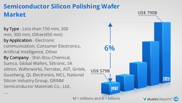
The outlook for the Global Semiconductor Silicon Polishing Wafer Market is promising, with significant growth anticipated over the coming years. In 2022, the global semiconductor market was valued at approximately $579 billion, and it is projected to reach $790 billion by 2029, reflecting a compound annual growth rate (CAGR) of 6% during the forecast period. This growth is driven by several factors, including the increasing demand for semiconductors in various applications, such as consumer electronics, automotive, telecommunications, and artificial intelligence. As technology continues to advance, the need for more powerful, efficient, and cost-effective semiconductor solutions is expected to rise, further fueling the market's expansion. Additionally, the ongoing development of new technologies, such as 5G, the Internet of Things (IoT), and advanced driver-assistance systems (ADAS), is expected to create new opportunities for the semiconductor industry, driving demand for high-quality silicon wafers. As a result, companies within the Global Semiconductor Silicon Polishing Wafer Market are likely to continue investing in research and development to enhance wafer quality, production efficiency, and sustainability, ensuring they remain competitive in this rapidly evolving industry.
| Report Metric | Details |
| Report Name | Semiconductor Silicon Polishing Wafer Market |
| Accounted market size in year | US$ 579 billion |
| Forecasted market size in 2029 | US$ 790 billion |
| CAGR | 6% |
| Base Year | year |
| Forecasted years | 2025 - 2029 |
| by Type |
|
| by Application |
|
| Production by Region |
|
| Consumption by Region |
|
| By Company | Shin-Etsu Chemical, Sumco, Global Wafers, Siltronic, SK siltron, Waferworks, Ferrotec, AST, Gritek, Guosheng, QL Electronics, MCL, National Silicon Industry Group, GRINM Semiconductor Materials Co., Ltd., ThinkonSemi, Tianjin Zhonghuan Semiconducto, Hangzhou Leon Dongxin Microelectronics, Wafer Technology, Hangzhou Zhongxin Wafer Semiconductor, Tianjin Zhongjing Semiconductor Materials Co., Ltd., Suzhou New Micron Nano Technology, ESWIN |
| Forecast units | USD million in value |
| Report coverage | Revenue and volume forecast, company share, competitive landscape, growth factors and trends |


