What is Global AlN Ceramics for Semiconductors Market?
The Global AlN Ceramics for Semiconductors Market is a specialized segment within the broader semiconductor industry, focusing on the use of aluminum nitride (AlN) ceramics. AlN ceramics are highly valued for their exceptional thermal conductivity, electrical insulation properties, and mechanical strength, making them ideal for various applications in semiconductor manufacturing. These ceramics are used in environments where high thermal management and electrical insulation are crucial, such as in power electronics, LED lighting, and RF components. The market for AlN ceramics is driven by the increasing demand for high-performance electronic devices and the ongoing miniaturization of semiconductor components. As technology advances, the need for materials that can efficiently dissipate heat and provide reliable electrical insulation becomes more critical, positioning AlN ceramics as a key material in the semiconductor industry. The market is characterized by continuous research and development efforts to enhance the properties of AlN ceramics and expand their applications, ensuring they meet the evolving needs of the semiconductor sector. This market is expected to grow steadily as the demand for advanced electronic devices continues to rise globally.
AlN Ceramic Heater, AlN Ceramic ESC, Others in the Global AlN Ceramics for Semiconductors Market:
AlN Ceramic Heaters are a significant component of the Global AlN Ceramics for Semiconductors Market. These heaters are designed to provide rapid and uniform heating, which is essential in semiconductor processing. The high thermal conductivity of AlN ceramics allows for efficient heat transfer, ensuring that the heaters can quickly reach and maintain the desired temperatures. This is particularly important in processes like chemical vapor deposition and epitaxial growth, where precise temperature control is crucial for achieving high-quality semiconductor layers. AlN Ceramic Heaters are also valued for their durability and resistance to thermal shock, making them suitable for use in demanding manufacturing environments. Additionally, their electrical insulation properties ensure that they can be used safely in applications where electrical interference must be minimized. AlN Ceramic Electrostatic Chucks (ESCs) are another critical application within this market. ESCs are used to hold semiconductor wafers in place during processing, using electrostatic forces to secure the wafer without the need for mechanical clamping. The use of AlN ceramics in ESCs provides several advantages, including excellent thermal management and electrical insulation. These properties help maintain the integrity of the wafer during processing, reducing the risk of damage and improving yield rates. AlN Ceramic ESCs are particularly beneficial in processes that require high-temperature stability and precise control, such as plasma etching and ion implantation. The use of AlN ceramics in ESCs also contributes to the overall efficiency and reliability of semiconductor manufacturing processes. Beyond heaters and ESCs, AlN ceramics find applications in various other components within the semiconductor industry. For instance, they are used in substrates for power electronics, where their thermal and electrical properties help improve device performance and reliability. AlN ceramics are also employed in RF components, where their ability to handle high frequencies and power levels is crucial. In LED lighting, AlN ceramics are used as substrates and heat sinks, helping to manage the heat generated by the LEDs and extend their lifespan. The versatility of AlN ceramics makes them an attractive choice for a wide range of applications, and ongoing research and development efforts continue to expand their potential uses. As the semiconductor industry evolves, the demand for materials that can meet the stringent requirements of advanced manufacturing processes will continue to drive the growth of the Global AlN Ceramics for Semiconductors Market.
Lithography, Etching, Thin Film Deposition, Others in the Global AlN Ceramics for Semiconductors Market:
The usage of Global AlN Ceramics for Semiconductors Market in lithography is pivotal due to the material's ability to withstand high temperatures and provide excellent thermal management. Lithography, a process used to transfer patterns onto semiconductor wafers, requires precise control of temperature and exposure to light. AlN ceramics, with their high thermal conductivity, ensure that the heat generated during the lithography process is efficiently dissipated, preventing any distortion of the patterns. This results in higher precision and accuracy in the manufacturing of semiconductor devices. In etching, AlN ceramics play a crucial role by providing a stable and inert environment for the removal of material from the wafer surface. The chemical resistance of AlN ceramics ensures that they can withstand the harsh chemicals used in etching processes, maintaining their integrity and performance over time. This durability is essential for achieving consistent and reliable results in semiconductor manufacturing. Thin film deposition, another critical area in semiconductor production, benefits from the use of AlN ceramics due to their excellent thermal and electrical properties. During thin film deposition, materials are deposited onto a substrate to form thin layers, which are essential for the functionality of semiconductor devices. AlN ceramics provide a stable and uniform surface for deposition, ensuring that the thin films adhere properly and maintain their desired properties. The thermal conductivity of AlN ceramics also helps manage the heat generated during deposition, preventing any damage to the substrate or the thin films. Beyond these specific applications, AlN ceramics are used in various other areas within the semiconductor industry. Their versatility and performance make them suitable for use in components such as heat sinks, substrates, and insulators, where their thermal and electrical properties contribute to the overall efficiency and reliability of semiconductor devices. As the demand for advanced electronic devices continues to grow, the role of AlN ceramics in semiconductor manufacturing will become increasingly important, driving further innovation and development in this field.
Global AlN Ceramics for Semiconductors Market Outlook:
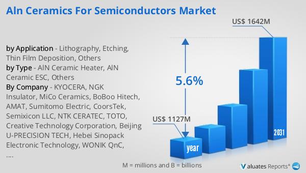
In 2024, the global market for AlN Ceramics for Semiconductors was valued at approximately $1,127 million. This market is anticipated to expand significantly, reaching an estimated size of $1,642 million by 2031. This growth trajectory represents a compound annual growth rate (CAGR) of 5.6% over the forecast period. The steady increase in market size reflects the rising demand for AlN ceramics, driven by their critical role in semiconductor manufacturing. As the semiconductor industry continues to evolve, the need for materials that offer superior thermal management and electrical insulation becomes more pronounced. AlN ceramics, with their unique properties, are well-positioned to meet these demands, supporting the production of high-performance electronic devices. The projected growth of the AlN Ceramics for Semiconductors Market underscores the importance of ongoing research and development efforts to enhance the properties of these materials and expand their applications. As technology advances and the demand for advanced electronic devices continues to rise, the market for AlN ceramics is expected to grow, providing opportunities for innovation and development in the semiconductor industry.
| Report Metric | Details |
| Report Name | AlN Ceramics for Semiconductors Market |
| Accounted market size in year | US$ 1127 million |
| Forecasted market size in 2031 | US$ 1642 million |
| CAGR | 5.6% |
| Base Year | year |
| Forecasted years | 2025 - 2031 |
| by Type |
|
| by Application |
|
| Production by Region |
|
| Consumption by Region |
|
| By Company | KYOCERA, NGK Insulator, MiCo Ceramics, BoBoo Hitech, AMAT, Sumitomo Electric, CoorsTek, Semixicon LLC, NTK CERATEC, TOTO, Creative Technology Corporation, Beijing U-PRECISION TECH, Hebei Sinopack Electronic Technology, WONIK QnC, Suzhou Kematek, Zhongshan Taniss |
| Forecast units | USD million in value |
| Report coverage | Revenue and volume forecast, company share, competitive landscape, growth factors and trends |


