Tuesday, March 4, 2025

Global Cu Electroplating Material Market Research Report 2025

What is Global Cu Electroplating Material Market?

The Global Cu Electroplating Material Market refers to the worldwide industry focused on the production and distribution of copper electroplating materials. These materials are essential in the process of electroplating, where a thin layer of copper is deposited onto the surface of a substrate, typically to enhance its appearance, improve corrosion resistance, or increase electrical conductivity. Copper electroplating is widely used across various industries, including electronics, automotive, and general manufacturing. The market for these materials is driven by the growing demand for electronic devices, advancements in semiconductor technology, and the need for durable and efficient components in various applications. As industries continue to innovate and expand, the demand for high-quality copper electroplating materials is expected to rise, making this market a critical component of the global manufacturing landscape. The market is characterized by a diverse range of products, including copper sulfate, copper anodes, and various additives that enhance the electroplating process. Companies operating in this market are continually investing in research and development to improve the efficiency and environmental sustainability of their products, ensuring they meet the evolving needs of their customers.

Cu Electroplating Material Market

Organic, Inorganic in the Global Cu Electroplating Material Market:

In the Global Cu Electroplating Material Market, materials are primarily categorized into organic and inorganic types, each with distinct properties and applications. Organic copper electroplating materials typically involve the use of organic additives that enhance the plating process. These additives can improve the brightness, leveling, and overall quality of the copper deposit. Organic materials are often preferred in applications where a high degree of precision and aesthetic quality is required, such as in the production of decorative items or intricate electronic components. The use of organic additives can also help in reducing the internal stress of the plated layer, thereby enhancing the durability and performance of the final product. On the other hand, inorganic copper electroplating materials are based on inorganic compounds, such as copper sulfate, which is one of the most commonly used copper salts in electroplating. Inorganic materials are typically used in applications where high conductivity and corrosion resistance are paramount, such as in the production of electrical connectors and circuit boards. The choice between organic and inorganic materials often depends on the specific requirements of the application, including factors such as cost, environmental impact, and desired properties of the plated layer. In recent years, there has been a growing emphasis on developing environmentally friendly electroplating materials, leading to innovations in both organic and inorganic categories. For instance, researchers are exploring the use of biodegradable organic additives and more efficient inorganic compounds that reduce waste and energy consumption. This trend is driven by increasing regulatory pressures and consumer demand for sustainable manufacturing practices. As a result, companies in the Global Cu Electroplating Material Market are investing heavily in research and development to create products that not only meet performance standards but also align with environmental goals. The competition between organic and inorganic materials is also influenced by technological advancements in related fields, such as nanotechnology and surface engineering. These advancements are opening up new possibilities for enhancing the properties of electroplated layers, such as increased hardness, improved adhesion, and enhanced thermal stability. As the market continues to evolve, the interplay between organic and inorganic materials will likely shape the future of copper electroplating, with each category offering unique advantages and challenges. Ultimately, the choice of material will depend on a careful consideration of the specific needs of the application, as well as broader industry trends and regulatory requirements.

General Hardware, Semiconductor, Others in the Global Cu Electroplating Material Market:

The Global Cu Electroplating Material Market finds extensive usage in various sectors, including general hardware, semiconductors, and other industries. In the realm of general hardware, copper electroplating is employed to enhance the durability and aesthetic appeal of metal components. This includes items such as fasteners, tools, and decorative hardware, where a copper-plated finish can provide both corrosion resistance and a visually appealing surface. The use of copper electroplating in general hardware is driven by the need for long-lasting and reliable components that can withstand harsh environmental conditions. In the semiconductor industry, copper electroplating plays a crucial role in the fabrication of integrated circuits and other electronic components. Copper's excellent electrical conductivity makes it an ideal material for creating the intricate wiring and connections required in modern electronic devices. The demand for copper electroplating materials in this sector is fueled by the rapid advancement of semiconductor technology and the increasing complexity of electronic devices. As devices become smaller and more powerful, the precision and quality of copper electroplating become even more critical. Beyond general hardware and semiconductors, copper electroplating materials are also used in a variety of other applications. This includes the automotive industry, where copper-plated components are used in electrical systems and decorative trims. The aerospace industry also utilizes copper electroplating for its ability to provide reliable electrical connections and protect components from corrosion. Additionally, copper electroplating is used in the production of consumer goods, such as jewelry and household items, where it provides an attractive and durable finish. The versatility of copper electroplating materials makes them an essential component in a wide range of industries, each with its unique requirements and challenges. As the Global Cu Electroplating Material Market continues to grow, the development of new applications and technologies will likely drive further innovation and expansion in this field.

Global Cu Electroplating Material Market Outlook:

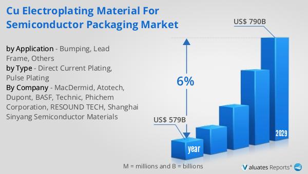
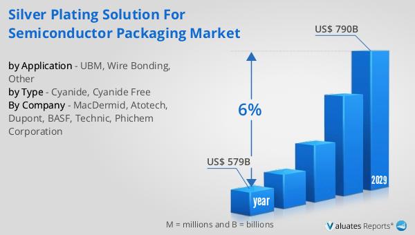
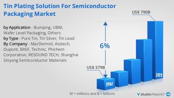
The global semiconductor market, which was valued at approximately $579 billion in 2022, is anticipated to reach around $790 billion by 2029, reflecting a compound annual growth rate (CAGR) of 6% over the forecast period. This growth is indicative of the increasing demand for semiconductors across various industries, driven by technological advancements and the proliferation of electronic devices. The semiconductor industry is a critical component of the global economy, underpinning the development of a wide range of products, from consumer electronics to industrial machinery. The projected growth in the semiconductor market is expected to have a significant impact on related industries, including the Global Cu Electroplating Material Market. As the demand for semiconductors rises, so too does the need for high-quality copper electroplating materials, which are essential in the manufacturing of semiconductor components. The growth of the semiconductor market is also likely to spur innovation and investment in the development of new electroplating technologies and materials, as companies seek to meet the evolving needs of their customers. This dynamic interplay between the semiconductor and electroplating markets highlights the interconnected nature of modern manufacturing and the importance of continued research and development in these fields.


Report Metric Details
Report Name Cu Electroplating Material Market
Accounted market size in year US$ 579 billion
Forecasted market size in 2029 US$ 790 billion
CAGR 6%
Base Year year
Forecasted years 2025 - 2029
by Type
  • Organic
  • Inorganic
by Application
  • General Hardware
  • Semiconductor
  • Others
Production by Region
  • North America
  • Europe
  • China
  • Japan
Consumption by Region
  • North America (United States, Canada)
  • Europe (Germany, France, UK, Italy, Russia)
  • Asia-Pacific (China, Japan, South Korea, Taiwan)
  • Southeast Asia (India)
  • Latin America (Mexico, Brazil)
By Company DuPont, BASF, Shanghai Sinyang Semiconductor Materials, ADEKA, Merck KGaA, Atotech, RESOUND TECH, PhiChem
Forecast units USD million in value
Report coverage Revenue and volume forecast, company share, competitive landscape, growth factors and trends

Global Cu Electroplating Material for Semiconductor Packaging Market Research Report 2025

What is Global Cu Electroplating Material for Semiconductor Packaging Market?

The Global Cu Electroplating Material for Semiconductor Packaging Market is a specialized segment within the broader semiconductor industry, focusing on the use of copper (Cu) electroplating materials in the packaging of semiconductors. This market is crucial because copper is widely used in semiconductor packaging due to its excellent electrical conductivity, thermal performance, and reliability. In semiconductor packaging, electroplating is a process where a thin layer of copper is deposited onto a substrate to create electrical connections and improve the overall performance of the semiconductor device. The demand for Cu electroplating materials is driven by the increasing complexity and miniaturization of semiconductor devices, which require more efficient and reliable packaging solutions. As technology advances, the need for high-performance materials like copper in semiconductor packaging continues to grow, making this market an essential component of the global semiconductor industry. The market's growth is also influenced by the rising demand for consumer electronics, automotive electronics, and other applications that rely on advanced semiconductor technologies. Overall, the Global Cu Electroplating Material for Semiconductor Packaging Market plays a vital role in supporting the development and production of cutting-edge semiconductor devices.

Cu Electroplating Material for Semiconductor Packaging Market

Direct Current Plating, Pulse Plating in the Global Cu Electroplating Material for Semiconductor Packaging Market:

Direct Current (DC) Plating and Pulse Plating are two prominent techniques used in the Global Cu Electroplating Material for Semiconductor Packaging Market. DC Plating is a traditional method where a constant direct current is applied to deposit copper onto a substrate. This technique is straightforward and cost-effective, making it widely used in various applications. However, DC Plating can sometimes lead to issues such as uneven deposition and poor surface quality, especially when dealing with complex geometries or high aspect ratio features. To address these challenges, Pulse Plating has emerged as an alternative technique. Pulse Plating involves the application of current in pulses, allowing for better control over the deposition process. By adjusting the pulse duration and frequency, manufacturers can achieve more uniform and dense copper layers, even on intricate structures. This method also helps in reducing defects and improving the overall quality of the electroplated layer. In the context of semiconductor packaging, both DC and Pulse Plating have their advantages and limitations. DC Plating is often preferred for simpler applications where cost is a major consideration, while Pulse Plating is favored for more demanding applications that require high precision and quality. The choice between these two techniques depends on various factors, including the specific requirements of the semiconductor device, the complexity of the packaging design, and the desired performance characteristics. As the semiconductor industry continues to evolve, the demand for advanced electroplating techniques like Pulse Plating is expected to increase, driven by the need for more efficient and reliable packaging solutions. Overall, both DC and Pulse Plating play a crucial role in the Global Cu Electroplating Material for Semiconductor Packaging Market, enabling the production of high-performance semiconductor devices that meet the growing demands of various industries.

Bumping, Lead Frame, Others in the Global Cu Electroplating Material for Semiconductor Packaging Market:

The usage of Global Cu Electroplating Material for Semiconductor Packaging Market is significant in several key areas, including Bumping, Lead Frame, and Others. In the context of Bumping, copper electroplating is used to create small bumps on the surface of semiconductor wafers. These bumps serve as interconnects that facilitate the connection between the semiconductor die and the package substrate. Copper is preferred for bumping due to its excellent electrical conductivity and mechanical strength, which help improve the performance and reliability of the final semiconductor device. The process of copper bumping involves depositing a layer of copper onto the wafer, followed by a series of additional steps to form the bumps. This technique is widely used in advanced packaging technologies such as flip-chip and wafer-level packaging, which require high-density interconnects and precise control over the bumping process. In the area of Lead Frame, copper electroplating is used to enhance the performance and reliability of lead frames, which are metal structures that provide mechanical support and electrical connections for semiconductor devices. Copper plating on lead frames helps improve their thermal and electrical conductivity, ensuring efficient heat dissipation and reliable electrical performance. This is particularly important in high-power applications where efficient heat management is critical to prevent device failure. Additionally, copper-plated lead frames offer better corrosion resistance and mechanical strength, contributing to the overall durability and longevity of the semiconductor package. Beyond Bumping and Lead Frame, copper electroplating is also used in other areas of semiconductor packaging, such as through-silicon vias (TSVs) and redistribution layers (RDLs). In these applications, copper is used to create vertical interconnects and fine wiring patterns that enable the integration of multiple semiconductor dies into a single package. The use of copper in these applications helps improve the electrical performance and integration density of the final package, supporting the development of more compact and efficient semiconductor devices. Overall, the Global Cu Electroplating Material for Semiconductor Packaging Market plays a crucial role in enabling the production of advanced semiconductor packages that meet the demands of modern electronic devices.

Global Cu Electroplating Material for Semiconductor Packaging Market Outlook:

The outlook for the Global Cu Electroplating Material for Semiconductor Packaging Market is closely tied to the broader semiconductor industry, which was valued at approximately $579 billion in 2022. This market is projected to grow to $790 billion by 2029, reflecting a compound annual growth rate (CAGR) of 6% over the forecast period. This growth is driven by several factors, including the increasing demand for consumer electronics, automotive electronics, and other applications that rely on advanced semiconductor technologies. As the semiconductor industry continues to expand, the need for efficient and reliable packaging solutions becomes more critical, driving the demand for copper electroplating materials. The use of copper in semiconductor packaging offers several advantages, including excellent electrical conductivity, thermal performance, and mechanical strength, making it an ideal choice for various packaging applications. Additionally, the ongoing trend towards miniaturization and increased integration density in semiconductor devices further fuels the demand for high-performance packaging materials like copper. As a result, the Global Cu Electroplating Material for Semiconductor Packaging Market is expected to experience significant growth in the coming years, supported by the continued advancements in semiconductor technology and the increasing complexity of electronic devices. Overall, the market outlook for copper electroplating materials in semiconductor packaging is positive, with strong growth prospects driven by the evolving needs of the semiconductor industry.


Report Metric Details
Report Name Cu Electroplating Material for Semiconductor Packaging Market
Accounted market size in year US$ 579 billion
Forecasted market size in 2029 US$ 790 billion
CAGR 6%
Base Year year
Forecasted years 2025 - 2029
by Type
  • Direct Current Plating
  • Pulse Plating
by Application
  • Bumping
  • Lead Frame
  • Others
Production by Region
  • North America
  • Europe
  • China
  • Japan
Consumption by Region
  • North America (United States, Canada)
  • Europe (Germany, France, UK, Italy, Russia)
  • Asia-Pacific (China, Japan, South Korea, Taiwan)
  • Southeast Asia (India)
  • Latin America (Mexico, Brazil)
By Company MacDermid, Atotech, Dupont, BASF, Technic, Phichem Corporation, RESOUND TECH, Shanghai Sinyang Semiconductor Materials
Forecast units USD million in value
Report coverage Revenue and volume forecast, company share, competitive landscape, growth factors and trends

Global Au Plating Solution for Semiconductor Packaging Market Research Report 2025

What is Global Au Plating Solution for Semiconductor Packaging Market?

The Global Au Plating Solution for Semiconductor Packaging Market is a specialized segment within the broader semiconductor industry, focusing on the use of gold (Au) plating solutions in the packaging of semiconductor devices. This market is crucial because gold plating is widely used in semiconductor packaging due to its excellent conductivity, corrosion resistance, and ability to form reliable connections. In semiconductor packaging, gold plating is applied to various components to ensure efficient electrical connections and protect against environmental factors that could degrade performance. The market encompasses a range of products and technologies designed to optimize the plating process, improve the quality of the plated layer, and enhance the overall performance of semiconductor devices. As the demand for advanced electronic devices continues to grow, the need for high-quality semiconductor packaging solutions, including gold plating, is expected to increase. This market is driven by technological advancements, increasing demand for miniaturized and high-performance electronic devices, and the need for reliable and durable packaging solutions. Companies operating in this market are focused on developing innovative plating solutions that meet the evolving needs of the semiconductor industry, ensuring that devices are both efficient and long-lasting.

Au Plating Solution for Semiconductor Packaging Market

Cyanide, Cyanide Free in the Global Au Plating Solution for Semiconductor Packaging Market:

Cyanide-based and cyanide-free solutions are two primary types of gold plating solutions used in the semiconductor packaging market. Cyanide-based solutions have been traditionally used due to their effectiveness in depositing gold layers with excellent adhesion and uniformity. These solutions typically contain potassium gold cyanide as the gold source, which is known for its stability and ability to produce high-quality gold deposits. However, the use of cyanide poses significant environmental and safety concerns due to its toxicity. Handling and disposal of cyanide-based solutions require strict regulatory compliance and safety measures to prevent environmental contamination and health risks to workers. Despite these challenges, cyanide-based solutions remain popular in the industry due to their proven performance and cost-effectiveness. On the other hand, cyanide-free solutions have emerged as a safer and more environmentally friendly alternative. These solutions use non-toxic chemicals to deposit gold, reducing the environmental impact and health risks associated with cyanide. Cyanide-free solutions are gaining traction in the market as companies seek to adopt more sustainable practices and comply with stringent environmental regulations. They offer comparable performance to cyanide-based solutions, making them an attractive option for semiconductor manufacturers looking to minimize their environmental footprint. The shift towards cyanide-free solutions is driven by increasing awareness of environmental issues, regulatory pressures, and the growing demand for sustainable manufacturing processes. Companies are investing in research and development to improve the performance and cost-effectiveness of cyanide-free solutions, ensuring they meet the high standards required in semiconductor packaging. As the industry continues to evolve, the adoption of cyanide-free solutions is expected to increase, driven by the need for safer and more sustainable plating processes. Both cyanide-based and cyanide-free solutions play a critical role in the semiconductor packaging market, offering different benefits and challenges. The choice between the two depends on various factors, including performance requirements, environmental considerations, and regulatory compliance. Companies must carefully evaluate these factors to select the most suitable plating solution for their specific needs. As the market continues to grow, the development of innovative and sustainable plating solutions will be essential to meet the demands of the semiconductor industry and ensure the continued advancement of electronic devices.

Bumping, Lead Frame, Others in the Global Au Plating Solution for Semiconductor Packaging Market:

The Global Au Plating Solution for Semiconductor Packaging Market finds its application in several key areas, including bumping, lead frame, and other specialized uses. In bumping, gold plating is used to create small bumps on semiconductor wafers, which serve as connection points for flip-chip packaging. This process is critical for ensuring reliable electrical connections and mechanical stability in advanced semiconductor devices. Gold's excellent conductivity and resistance to oxidation make it an ideal material for bumping applications, where maintaining signal integrity and device performance is crucial. The use of gold plating in bumping helps to enhance the performance and longevity of semiconductor devices, making it a vital component of modern electronic manufacturing. In lead frame applications, gold plating is used to coat the metal frames that support and connect semiconductor chips within a package. The lead frame serves as the primary interface between the semiconductor device and the external circuitry, making it essential for ensuring efficient electrical connections. Gold plating on lead frames provides excellent corrosion resistance and conductivity, ensuring that the connections remain reliable over the device's lifespan. This is particularly important in harsh environments where exposure to moisture and other corrosive elements can degrade performance. The use of gold plating in lead frames helps to improve the overall reliability and performance of semiconductor packages, making it a critical component of the packaging process. Beyond bumping and lead frames, gold plating solutions are used in various other applications within the semiconductor packaging market. These include wire bonding, where gold-plated wires are used to connect semiconductor chips to the lead frame or substrate. Gold's excellent conductivity and bondability make it an ideal choice for wire bonding applications, ensuring reliable connections and high performance. Additionally, gold plating is used in the production of connectors and contacts, where its resistance to corrosion and wear ensures long-lasting performance. The versatility and reliability of gold plating make it an essential component of the semiconductor packaging process, supporting the development of advanced electronic devices and systems. As the demand for high-performance and miniaturized electronic devices continues to grow, the use of gold plating solutions in semiconductor packaging is expected to increase, driving innovation and advancement in the industry.

Global Au Plating Solution for Semiconductor Packaging Market Outlook:

In 2022, the global semiconductor market was valued at approximately $579 billion, and it is anticipated to reach around $790 billion by 2029, reflecting a compound annual growth rate (CAGR) of 6% over the forecast period. This growth trajectory underscores the increasing demand for semiconductors, driven by advancements in technology and the proliferation of electronic devices across various sectors. The semiconductor industry plays a pivotal role in the global economy, powering everything from consumer electronics to industrial machinery and automotive systems. As technology continues to evolve, the demand for more sophisticated and efficient semiconductor solutions is expected to rise, fueling market growth. The projected increase in market value highlights the importance of innovation and investment in the semiconductor sector, as companies strive to meet the growing needs of consumers and industries worldwide. This growth is also indicative of the expanding applications of semiconductors, as they become integral to emerging technologies such as artificial intelligence, the Internet of Things (IoT), and 5G networks. As the market continues to expand, companies in the semiconductor industry will need to focus on developing cutting-edge technologies and solutions to maintain their competitive edge and capitalize on the opportunities presented by this dynamic and rapidly evolving market.


Report Metric Details
Report Name Au Plating Solution for Semiconductor Packaging Market
Accounted market size in year US$ 579 billion
Forecasted market size in 2029 US$ 790 billion
CAGR 6%
Base Year year
Forecasted years 2025 - 2029
by Type
  • Cyanide
  • Cyanide Free
by Application
  • Bumping
  • Lead Frame
  • Others
Production by Region
  • North America
  • Europe
  • China
  • Japan
Consumption by Region
  • North America (United States, Canada)
  • Europe (Germany, France, UK, Italy, Russia)
  • Asia-Pacific (China, Japan, South Korea, Taiwan)
  • Southeast Asia (India)
  • Latin America (Mexico, Brazil)
By Company MacDermid, Atotech, Dupont, Technic
Forecast units USD million in value
Report coverage Revenue and volume forecast, company share, competitive landscape, growth factors and trends

Global Silver Plating Solution for Semiconductor Packaging Market Research Report 2025

What is Global Silver Plating Solution for Semiconductor Packaging Market?

The Global Silver Plating Solution for Semiconductor Packaging Market is a specialized segment within the semiconductor industry that focuses on the application of silver plating solutions to semiconductor components. Silver plating is a critical process in semiconductor packaging, which involves encasing semiconductor devices to protect them from physical damage and corrosion while ensuring efficient electrical conductivity. This market is driven by the increasing demand for advanced electronic devices, which require reliable and efficient semiconductor components. Silver plating solutions are used to enhance the performance and longevity of these components by providing a conductive and corrosion-resistant surface. The market encompasses various types of silver plating solutions, including those based on cyanide and cyanide-free formulations, each offering distinct advantages and applications. As the semiconductor industry continues to grow, driven by technological advancements and the proliferation of electronic devices, the demand for high-quality silver plating solutions is expected to rise, making this market an essential part of the global semiconductor supply chain.

Silver Plating Solution for Semiconductor Packaging Market

Cyanide, Cyanide Free in the Global Silver Plating Solution for Semiconductor Packaging Market:

Cyanide-based and cyanide-free silver plating solutions are two primary types of formulations used in the Global Silver Plating Solution for Semiconductor Packaging Market. Cyanide-based solutions have been traditionally used due to their effectiveness in providing a uniform and high-quality silver coating. These solutions are known for their excellent throwing power, which ensures even coverage on complex geometries, and their ability to produce a bright and smooth finish. However, the use of cyanide poses significant environmental and safety concerns due to its toxic nature. Handling and disposal of cyanide-based solutions require stringent safety measures and regulatory compliance, which can increase operational costs and complexity for manufacturers. On the other hand, cyanide-free silver plating solutions have emerged as a safer and more environmentally friendly alternative. These solutions eliminate the risks associated with cyanide, making them easier to handle and dispose of. Cyanide-free formulations often use alternative complexing agents, such as thiosulfate or sulfite, to achieve similar plating quality. While they may not always match the performance of cyanide-based solutions in terms of brightness and smoothness, ongoing research and development efforts are focused on improving their effectiveness. The choice between cyanide and cyanide-free solutions often depends on the specific requirements of the application, regulatory considerations, and the manufacturer's commitment to sustainability. As the industry moves towards greener practices, the adoption of cyanide-free solutions is expected to increase, driven by both regulatory pressures and consumer demand for environmentally responsible products. This shift presents opportunities for innovation and growth within the market, as companies invest in developing advanced cyanide-free formulations that meet the high standards of the semiconductor industry.

UBM, Wire Bonding, Other in the Global Silver Plating Solution for Semiconductor Packaging Market:

The Global Silver Plating Solution for Semiconductor Packaging Market finds its applications in various areas, including Under Bump Metallization (UBM), wire bonding, and other specialized uses. In UBM, silver plating is used to create a conductive layer between the semiconductor die and the substrate. This layer is crucial for ensuring reliable electrical connections and mechanical stability in flip-chip packages. Silver's excellent conductivity and resistance to oxidation make it an ideal choice for UBM applications, where maintaining signal integrity and minimizing resistance is critical. In wire bonding, silver plating is used to enhance the bondability of semiconductor components. The silver layer provides a clean and conductive surface for wire bonds, ensuring strong and reliable connections. This is particularly important in high-frequency and high-power applications, where any increase in resistance can lead to performance degradation. Silver's ability to withstand high temperatures and its excellent thermal conductivity also contribute to its suitability for wire bonding applications. Beyond UBM and wire bonding, silver plating solutions are used in other areas of semiconductor packaging, such as lead frames and connectors. In these applications, silver plating provides corrosion resistance and enhances solderability, ensuring long-term reliability and performance. The versatility of silver plating solutions makes them an essential component in the semiconductor packaging process, supporting the development of advanced electronic devices across various industries. As the demand for smaller, faster, and more efficient electronic devices continues to grow, the role of silver plating solutions in semiconductor packaging is expected to become increasingly important, driving innovation and growth in this market segment.

Global Silver Plating Solution for Semiconductor Packaging Market Outlook:

The global semiconductor market, valued at approximately $579 billion in 2022, is on a growth trajectory, with projections indicating it could reach around $790 billion by 2029. This growth is expected to occur at a compound annual growth rate (CAGR) of 6% over the forecast period. This expansion reflects the increasing demand for semiconductors, driven by advancements in technology and the proliferation of electronic devices across various sectors. The semiconductor industry is a cornerstone of modern technology, underpinning everything from consumer electronics to industrial applications. As the world becomes more interconnected and reliant on digital solutions, the demand for semiconductors is set to rise, fueling growth in related markets, including the Global Silver Plating Solution for Semiconductor Packaging Market. This market plays a crucial role in ensuring the reliability and performance of semiconductor components, which are essential for the functioning of electronic devices. As the semiconductor market grows, so too does the need for high-quality silver plating solutions that can meet the stringent requirements of modern electronic devices. This growth presents opportunities for innovation and development within the silver plating solution market, as companies strive to create advanced formulations that enhance the performance and longevity of semiconductor components.


Report Metric Details
Report Name Silver Plating Solution for Semiconductor Packaging Market
Accounted market size in year US$ 579 billion
Forecasted market size in 2029 US$ 790 billion
CAGR 6%
Base Year year
Forecasted years 2025 - 2029
by Type
  • Cyanide
  • Cyanide Free
by Application
  • UBM
  • Wire Bonding
  • Other
Production by Region
  • North America
  • Europe
  • China
  • Japan
Consumption by Region
  • North America (United States, Canada)
  • Europe (Germany, France, UK, Italy, Russia)
  • Asia-Pacific (China, Japan, South Korea, Taiwan)
  • Southeast Asia (India)
  • Latin America (Mexico, Brazil)
By Company MacDermid, Atotech, Dupont, BASF, Technic, Phichem Corporation
Forecast units USD million in value
Report coverage Revenue and volume forecast, company share, competitive landscape, growth factors and trends

Global Tin Plating Solution for Semiconductor Packaging Market Research Report 2025

What is Global Tin Plating Solution for Semiconductor Packaging Market?

The Global Tin Plating Solution for Semiconductor Packaging Market is a specialized segment within the broader semiconductor industry, focusing on the application of tin plating in semiconductor packaging. Tin plating is a crucial process that involves coating semiconductor components with a thin layer of tin to enhance their performance and longevity. This process is essential for protecting semiconductor devices from corrosion, improving solderability, and ensuring reliable electrical connections. The market for tin plating solutions is driven by the increasing demand for semiconductors in various applications, including consumer electronics, automotive, and industrial sectors. As technology advances, the need for more efficient and reliable semiconductor packaging solutions grows, making tin plating an indispensable part of the manufacturing process. The market is characterized by continuous innovation and development of new plating techniques to meet the evolving needs of the semiconductor industry. Companies operating in this market are focused on providing high-quality, cost-effective tin plating solutions that comply with environmental regulations and industry standards. The global tin plating solution market is poised for growth as the demand for semiconductors continues to rise, driven by technological advancements and the proliferation of electronic devices.

Tin Plating Solution for Semiconductor Packaging Market

Pure Tin, Tin Silver, Tin Lead in the Global Tin Plating Solution for Semiconductor Packaging Market:

In the Global Tin Plating Solution for Semiconductor Packaging Market, three primary types of tin plating are commonly used: Pure Tin, Tin Silver, and Tin Lead. Each of these has distinct properties and applications, catering to different needs within the semiconductor industry. Pure Tin plating is widely used due to its excellent solderability and corrosion resistance. It provides a reliable surface for soldering, which is crucial in semiconductor packaging. Pure Tin is also favored for its environmental friendliness, as it does not contain lead, making it compliant with RoHS (Restriction of Hazardous Substances) regulations. However, one of the challenges with Pure Tin is the potential for tin whisker growth, which can lead to short circuits. To mitigate this, manufacturers often employ additional processes or coatings to prevent whisker formation. Tin Silver plating, on the other hand, is known for its superior mechanical properties and thermal stability. The addition of silver enhances the plating's resistance to wear and improves its conductivity, making it suitable for high-performance applications. Tin Silver is often used in environments where components are subjected to high temperatures and mechanical stress. It also offers better resistance to tin whisker growth compared to Pure Tin, making it a preferred choice for critical applications. Tin Lead plating has been a traditional choice in the semiconductor industry due to its excellent solderability and resistance to whisker growth. The presence of lead in the alloy helps prevent the formation of tin whiskers, ensuring long-term reliability of the components. However, due to environmental concerns and regulatory restrictions, the use of Tin Lead plating has declined in recent years. Many manufacturers are transitioning to lead-free alternatives like Pure Tin and Tin Silver to comply with environmental regulations. Despite this, Tin Lead plating is still used in certain applications where its unique properties are required, and exemptions from regulations are granted. Each type of tin plating offers distinct advantages and challenges, and the choice of plating depends on the specific requirements of the semiconductor application. Manufacturers must carefully consider factors such as solderability, environmental impact, mechanical properties, and regulatory compliance when selecting a tin plating solution for semiconductor packaging.

Bumping, UBM, Wafer Level Packaging, Others in the Global Tin Plating Solution for Semiconductor Packaging Market:

The Global Tin Plating Solution for Semiconductor Packaging Market finds its application in several key areas, including Bumping, Under Bump Metallization (UBM), Wafer Level Packaging, and others. In the context of Bumping, tin plating is used to create small bumps on the surface of semiconductor wafers. These bumps serve as interconnects that facilitate the connection between the semiconductor die and the substrate or printed circuit board (PCB). Tin plating in bumping provides excellent solderability and ensures reliable electrical connections, which are critical for the performance of semiconductor devices. The use of tin plating in bumping is particularly important in flip-chip technology, where the die is mounted face-down on the substrate, requiring robust and reliable interconnects. Under Bump Metallization (UBM) is another area where tin plating plays a crucial role. UBM is a process that involves depositing a metal layer on the semiconductor wafer to enhance the adhesion and solderability of the bumps. Tin plating is often used in UBM to provide a solderable surface that ensures strong and reliable connections between the die and the substrate. The choice of tin plating in UBM depends on factors such as the type of solder used, the operating environment, and the specific requirements of the semiconductor application. Wafer Level Packaging (WLP) is an advanced packaging technology that involves packaging the semiconductor die at the wafer level, before it is diced into individual chips. Tin plating is used in WLP to provide a protective coating that enhances the solderability and reliability of the package. The use of tin plating in WLP helps improve the electrical performance of the package and ensures long-term reliability in various operating conditions. Other applications of tin plating in the semiconductor packaging market include lead frame plating, connector plating, and terminal plating. In these applications, tin plating provides corrosion resistance, enhances solderability, and ensures reliable electrical connections. The versatility and effectiveness of tin plating make it an essential component in the semiconductor packaging process, catering to a wide range of applications and requirements.

Global Tin Plating Solution for Semiconductor Packaging Market Outlook:

The outlook for the Global Tin Plating Solution for Semiconductor Packaging Market is closely tied to the overall growth of the semiconductor industry. In 2022, the global semiconductor market was valued at approximately US$ 579 billion. This market is projected to grow significantly, reaching an estimated value of US$ 790 billion by 2029. This growth represents a compound annual growth rate (CAGR) of 6% over the forecast period. The increasing demand for semiconductors in various applications, including consumer electronics, automotive, and industrial sectors, is a key driver of this growth. As technology continues to advance, the need for more efficient and reliable semiconductor packaging solutions becomes increasingly important. Tin plating solutions play a crucial role in enhancing the performance and longevity of semiconductor devices, making them an integral part of the manufacturing process. The market for tin plating solutions is expected to benefit from the overall growth of the semiconductor industry, as manufacturers seek high-quality, cost-effective solutions that comply with environmental regulations and industry standards. The continuous innovation and development of new plating techniques will further drive the growth of the tin plating solution market, ensuring its relevance and importance in the semiconductor industry.


Report Metric Details
Report Name Tin Plating Solution for Semiconductor Packaging Market
Accounted market size in year US$ 579 billion
Forecasted market size in 2029 US$ 790 billion
CAGR 6%
Base Year year
Forecasted years 2025 - 2029
by Type
  • Pure Tin
  • Tin Silver
  • Tin Lead
by Application
  • Bumping
  • UBM
  • Wafer Level Packaging
  • Others
Production by Region
  • North America
  • Europe
  • China
  • Japan
Consumption by Region
  • North America (United States, Canada)
  • Europe (Germany, France, UK, Italy, Russia)
  • Asia-Pacific (China, Japan, South Korea, Taiwan)
  • Southeast Asia (India)
  • Latin America (Mexico, Brazil)
By Company MacDermid, Atotech, Dupont, BASF, Technic, Phichem Corporation, RESOUND TECH, Shanghai Sinyang Semiconductor Materials
Forecast units USD million in value
Report coverage Revenue and volume forecast, company share, competitive landscape, growth factors and trends

Global Aerogel Material Market Research Report 2025

What is Global Aerogel Material Market?

The Global Aerogel Material Market is a fascinating sector within the materials industry, characterized by its unique properties and diverse applications. Aerogels are lightweight, porous materials derived from a gel, where the liquid component is replaced with gas, resulting in a solid with extremely low density and thermal conductivity. These materials are often referred to as "frozen smoke" due to their translucent appearance and are renowned for their exceptional insulating properties. The market for aerogel materials is driven by their increasing use in various industries, including oil and gas, construction, transportation, and aerospace, where their ability to provide superior insulation and reduce energy consumption is highly valued. As industries continue to seek sustainable and efficient solutions, the demand for aerogel materials is expected to grow, driven by advancements in manufacturing processes and the development of new applications. The market is also influenced by factors such as environmental regulations, technological innovations, and the need for energy-efficient materials, making it a dynamic and evolving sector with significant potential for growth and innovation.

Aerogel Material Market

Aerogel Felt, Powder, Others in the Global Aerogel Material Market:

Aerogel materials are available in various forms, including felt, powder, and other specialized types, each offering distinct advantages and applications. Aerogel felt is a flexible, blanket-like material that combines the thermal insulation properties of aerogels with the flexibility and ease of use of traditional insulation materials. This form is particularly popular in industries such as construction and oil and gas, where it is used to insulate pipes, tanks, and other equipment. The flexibility of aerogel felt allows it to be easily wrapped around complex shapes and surfaces, providing effective insulation while minimizing heat loss. Additionally, its lightweight nature makes it easy to handle and install, reducing labor costs and installation time. Aerogel powder, on the other hand, is a fine, granular form of aerogel that is often used as an additive in coatings, paints, and other materials to enhance their thermal insulation properties. This form is particularly useful in applications where a thin, lightweight layer of insulation is required, such as in aerospace and automotive industries. Aerogel powder can be mixed with other materials to create composites that offer improved thermal performance without adding significant weight or bulk. Other forms of aerogel materials include monolithic aerogels, which are solid blocks of aerogel used in specialized applications where maximum insulation is required. These monolithic forms are often used in scientific research and high-tech industries, where their unique properties can be fully utilized. The versatility of aerogel materials, combined with their exceptional insulating properties, makes them an attractive option for a wide range of applications, from industrial insulation to consumer products. As the demand for energy-efficient and sustainable materials continues to grow, the market for aerogel materials is expected to expand, driven by ongoing research and development efforts and the introduction of new and innovative products.

Oil And Gas, Building Insulation, Transportation, Aerospace And Defense Materials, Others in the Global Aerogel Material Market:

The Global Aerogel Material Market finds extensive usage across various sectors, each benefiting from the unique properties of aerogels. In the oil and gas industry, aerogel materials are primarily used for insulation purposes. Their ability to withstand extreme temperatures and resist moisture makes them ideal for insulating pipelines, storage tanks, and other equipment. This not only helps in maintaining the temperature of the transported materials but also reduces energy consumption and minimizes the risk of condensation and corrosion. In the building insulation sector, aerogels are used to enhance the thermal efficiency of buildings. Their lightweight and flexible nature allows them to be easily integrated into walls, roofs, and floors, providing superior insulation without adding significant weight or bulk. This helps in reducing energy costs and improving the overall energy efficiency of buildings. In the transportation industry, aerogel materials are used to improve the thermal insulation of vehicles, including cars, trucks, and trains. Their lightweight nature helps in reducing the overall weight of the vehicle, leading to improved fuel efficiency and reduced emissions. In the aerospace and defense sectors, aerogels are used in a variety of applications, including thermal insulation for spacecraft and aircraft, as well as in protective clothing and equipment for military personnel. Their ability to provide superior insulation while being lightweight and durable makes them an ideal choice for these demanding applications. Other sectors that benefit from the use of aerogel materials include electronics, where they are used to insulate sensitive components, and consumer products, where they are used to improve the thermal performance of items such as clothing and footwear. The versatility and effectiveness of aerogel materials make them a valuable resource in a wide range of industries, driving their demand and contributing to the growth of the Global Aerogel Material Market.

Global Aerogel Material Market Outlook:

The outlook for the Global Aerogel Material Market is promising, with significant growth expected in the coming years. In 2024, the market was valued at approximately US$ 597 million, and it is projected to reach around US$ 886 million by 2031. This growth represents a compound annual growth rate (CAGR) of 5.9% over the forecast period. This upward trend is driven by the increasing demand for energy-efficient and sustainable materials across various industries. As more sectors recognize the benefits of aerogel materials, including their superior insulation properties and lightweight nature, the market is expected to expand further. The growth is also supported by advancements in manufacturing technologies, which are making aerogel materials more accessible and affordable. Additionally, the growing focus on reducing carbon emissions and improving energy efficiency is likely to drive the adoption of aerogel materials in industries such as construction, transportation, and aerospace. As a result, the Global Aerogel Material Market is poised for significant growth, offering numerous opportunities for innovation and development in the coming years.


Report Metric Details
Report Name Aerogel Material Market
Accounted market size in year US$ 597 million
Forecasted market size in 2031 US$ 886 million
CAGR 5.9%
Base Year year
Forecasted years 2025 - 2031
by Type
  • Aerogel Felt
  • Powder
  • Others
by Application
  • Oil And Gas
  • Building Insulation
  • Transportation
  • Aerospace And Defense Materials
  • Others
Production by Region
  • North America
  • Europe
  • China
  • Japan
Consumption by Region
  • North America (United States, Canada)
  • Europe (Germany, France, UK, Italy, Russia)
  • Asia-Pacific (China, Japan, South Korea, Taiwan)
  • Southeast Asia (India)
  • Latin America (Mexico, Brazil)
By Company Aspen Aerogel, Cabotcorp, Aerogel Technologies, Nanuo, Alison Aerogel, Active Aerogels, Enersens, Jios Aerogel Corporation, Htwjjd, Agel-Tech, Aerogel UK, Nameite New Materials Technology, IBIH, Jinna Tech
Forecast units USD million in value
Report coverage Revenue and volume forecast, company share, competitive landscape, growth factors and trends

Global Sponge Titanium Market Research Report 2025

What is Global Sponge Titanium Market?

The Global Sponge Titanium Market is a crucial segment of the broader titanium industry, focusing on the production and distribution of sponge titanium, which is a porous form of titanium created during the initial stages of titanium processing. This market is vital because sponge titanium serves as the primary raw material for producing titanium metal and its alloys. Titanium is renowned for its exceptional strength-to-weight ratio, corrosion resistance, and ability to withstand extreme temperatures, making it indispensable in various high-performance applications. The demand for sponge titanium is driven by its extensive use in industries such as aerospace, defense, chemical processing, and power generation. As these industries continue to expand and innovate, the need for high-quality titanium materials grows, thereby fueling the sponge titanium market. Additionally, the market is influenced by factors such as technological advancements in production processes, fluctuations in raw material prices, and environmental regulations. The global sponge titanium market is characterized by a few key players who dominate production and supply, ensuring that the demand for this essential material is met efficiently. As industries evolve and new applications for titanium emerge, the sponge titanium market is poised for continued growth and development.

Sponge Titanium Market

Ti Above 99.7%, Ti 99.5~99.7%, Ti 99.3~99.5%, Ti Below 99.3% in the Global Sponge Titanium Market:

In the Global Sponge Titanium Market, titanium is categorized based on its purity levels, which significantly influence its applications and value. The highest purity level, Ti Above 99.7%, is highly sought after for its superior quality and performance characteristics. This grade is predominantly used in critical applications where the utmost reliability and strength are required, such as in aerospace components, medical implants, and high-end industrial equipment. Its exceptional corrosion resistance and mechanical properties make it ideal for environments that demand durability and precision. The next category, Ti 99.5~99.7%, offers a slightly lower purity but still maintains excellent performance for a wide range of applications. This grade is often utilized in industries where a balance between cost and performance is necessary, such as in chemical processing equipment and certain automotive parts. It provides a good compromise between high purity and economic feasibility, making it a popular choice for many manufacturers. Ti 99.3~99.5% represents a mid-range purity level that is suitable for less demanding applications where extreme conditions are not a primary concern. This grade is commonly used in consumer goods, construction materials, and general industrial applications where the benefits of titanium's strength and corrosion resistance are desired without the need for the highest purity. Finally, Ti Below 99.3% is the lowest purity level in the sponge titanium market, often used in applications where cost is a more significant factor than performance. This grade is typically found in non-critical components and products where the unique properties of titanium are beneficial but do not require the highest levels of purity. The varying purity levels of sponge titanium allow manufacturers to select the most appropriate grade for their specific needs, balancing performance requirements with cost considerations. As the demand for titanium continues to grow across various industries, the ability to tailor the purity of sponge titanium to meet specific application needs is a crucial factor in the market's ongoing development and success.

Aerospace and Defense, Chemicals, Ocean and Ship, Electric Power, Others in the Global Sponge Titanium Market:

The Global Sponge Titanium Market plays a pivotal role in several key industries, each benefiting from the unique properties of titanium. In the aerospace and defense sectors, titanium's high strength-to-weight ratio and excellent corrosion resistance make it an ideal material for aircraft components, missile systems, and spacecraft. Its ability to withstand extreme temperatures and harsh environments ensures the reliability and safety of critical systems, making it indispensable in these high-stakes applications. The chemical industry also relies heavily on sponge titanium, particularly for its resistance to corrosive substances. Titanium is used in the construction of reactors, heat exchangers, and other equipment that must endure aggressive chemical processes. Its durability and longevity reduce maintenance costs and downtime, making it a cost-effective choice for chemical manufacturers. In the ocean and shipbuilding industries, titanium's resistance to seawater corrosion is highly valued. It is used in the construction of ship hulls, propellers, and offshore structures, where exposure to saltwater and harsh marine conditions is a constant challenge. Titanium's lightweight nature also contributes to fuel efficiency and performance in marine vessels. The electric power industry benefits from titanium's ability to withstand high temperatures and corrosive environments, making it suitable for use in power plant components such as condensers and heat exchangers. Its reliability and long service life contribute to the efficient operation of power generation facilities. Beyond these primary industries, sponge titanium finds applications in various other sectors, including medical devices, automotive manufacturing, and consumer electronics. Its biocompatibility makes it ideal for medical implants and prosthetics, while its strength and lightweight properties enhance the performance of automotive and electronic products. As these industries continue to innovate and expand, the demand for sponge titanium is expected to grow, driven by the need for materials that offer superior performance and reliability. The versatility and adaptability of sponge titanium ensure its continued relevance and importance across a wide range of applications.

Global Sponge Titanium Market Outlook:

The global market for Sponge Titanium was valued at $2,550 million in 2024 and is anticipated to expand to a revised size of $3,233 million by 2031, reflecting a compound annual growth rate (CAGR) of 3.5% over the forecast period. This growth trajectory underscores the increasing demand for sponge titanium across various industries, driven by its unique properties and wide-ranging applications. Leading the charge in this market are prominent manufacturers such as AVISMA, UKTMP, and ZTMC, who collectively account for 31% of the industry's revenues. These companies are at the forefront of innovation and production, ensuring a steady supply of high-quality sponge titanium to meet global demand. Regionally, China stands out as the dominant player, contributing approximately 38% of the market's regional income. This significant share highlights China's robust industrial base and its strategic investments in the titanium sector. The country's focus on expanding its aerospace, defense, and chemical industries further fuels its demand for sponge titanium, solidifying its position as a key market leader. As the global economy continues to evolve, the sponge titanium market is poised for sustained growth, driven by technological advancements, increasing industrialization, and the ongoing pursuit of high-performance materials.


Report Metric Details
Report Name Sponge Titanium Market
Accounted market size in year US$ 2550 million
Forecasted market size in 2031 US$ 3233 million
CAGR 3.5%
Base Year year
Forecasted years 2025 - 2031
by Type
  • Ti Above 99.7%
  • Ti 99.5~99.7%
  • Ti 99.3~99.5%
  • Ti Below 99.3%
by Application
  • Aerospace and Defense
  • Chemicals
  • Ocean and Ship
  • Electric Power
  • Others
Production by Region
  • North America
  • Europe
  • China
  • Japan
Consumption by Region
  • North America (United States, Canada)
  • Europe (Germany, France, UK, Italy, Russia)
  • Asia-Pacific (China, Japan, South Korea, Taiwan)
  • Southeast Asia (India)
  • Latin America (Mexico, Brazil)
By Company AVISMA, UKTMP, ZTMC, Timet, ATI, OSAKA Titanium, Toho Titanium, Zunyi Titanium, Pangang Titanium, Luoyang Shuangrui Wanji Titanium, Chaoyang Jinda, Baotai Huashen, Yunnan Xinli, Chaoyang Baisheng, Anshan Hailiang, Shanxi Zhuofeng
Forecast units USD million in value
Report coverage Revenue and volume forecast, company share, competitive landscape, growth factors and trends

Global DPDT Type Rotary Gear Limit Switches Market Research Report 2025

What is Global DPDT Type Rotary Gear Limit Switches Market? The Global DPDT Type Rotary Gear Limit Switches Market refers to the worldwide ...