What is Global Cu Electroplating Material for Semiconductor Packaging Market?
The Global Cu Electroplating Material for Semiconductor Packaging Market is a specialized segment within the broader semiconductor industry, focusing on the use of copper (Cu) electroplating materials in the packaging of semiconductors. This market is crucial because copper is widely used in semiconductor packaging due to its excellent electrical conductivity, thermal performance, and reliability. In semiconductor packaging, electroplating is a process where a thin layer of copper is deposited onto a substrate to create electrical connections and improve the overall performance of the semiconductor device. The demand for Cu electroplating materials is driven by the increasing complexity and miniaturization of semiconductor devices, which require more efficient and reliable packaging solutions. As technology advances, the need for high-performance materials like copper in semiconductor packaging continues to grow, making this market an essential component of the global semiconductor industry. The market's growth is also influenced by the rising demand for consumer electronics, automotive electronics, and other applications that rely on advanced semiconductor technologies. Overall, the Global Cu Electroplating Material for Semiconductor Packaging Market plays a vital role in supporting the development and production of cutting-edge semiconductor devices.
Direct Current Plating, Pulse Plating in the Global Cu Electroplating Material for Semiconductor Packaging Market:
Direct Current (DC) Plating and Pulse Plating are two prominent techniques used in the Global Cu Electroplating Material for Semiconductor Packaging Market. DC Plating is a traditional method where a constant direct current is applied to deposit copper onto a substrate. This technique is straightforward and cost-effective, making it widely used in various applications. However, DC Plating can sometimes lead to issues such as uneven deposition and poor surface quality, especially when dealing with complex geometries or high aspect ratio features. To address these challenges, Pulse Plating has emerged as an alternative technique. Pulse Plating involves the application of current in pulses, allowing for better control over the deposition process. By adjusting the pulse duration and frequency, manufacturers can achieve more uniform and dense copper layers, even on intricate structures. This method also helps in reducing defects and improving the overall quality of the electroplated layer. In the context of semiconductor packaging, both DC and Pulse Plating have their advantages and limitations. DC Plating is often preferred for simpler applications where cost is a major consideration, while Pulse Plating is favored for more demanding applications that require high precision and quality. The choice between these two techniques depends on various factors, including the specific requirements of the semiconductor device, the complexity of the packaging design, and the desired performance characteristics. As the semiconductor industry continues to evolve, the demand for advanced electroplating techniques like Pulse Plating is expected to increase, driven by the need for more efficient and reliable packaging solutions. Overall, both DC and Pulse Plating play a crucial role in the Global Cu Electroplating Material for Semiconductor Packaging Market, enabling the production of high-performance semiconductor devices that meet the growing demands of various industries.
Bumping, Lead Frame, Others in the Global Cu Electroplating Material for Semiconductor Packaging Market:
The usage of Global Cu Electroplating Material for Semiconductor Packaging Market is significant in several key areas, including Bumping, Lead Frame, and Others. In the context of Bumping, copper electroplating is used to create small bumps on the surface of semiconductor wafers. These bumps serve as interconnects that facilitate the connection between the semiconductor die and the package substrate. Copper is preferred for bumping due to its excellent electrical conductivity and mechanical strength, which help improve the performance and reliability of the final semiconductor device. The process of copper bumping involves depositing a layer of copper onto the wafer, followed by a series of additional steps to form the bumps. This technique is widely used in advanced packaging technologies such as flip-chip and wafer-level packaging, which require high-density interconnects and precise control over the bumping process. In the area of Lead Frame, copper electroplating is used to enhance the performance and reliability of lead frames, which are metal structures that provide mechanical support and electrical connections for semiconductor devices. Copper plating on lead frames helps improve their thermal and electrical conductivity, ensuring efficient heat dissipation and reliable electrical performance. This is particularly important in high-power applications where efficient heat management is critical to prevent device failure. Additionally, copper-plated lead frames offer better corrosion resistance and mechanical strength, contributing to the overall durability and longevity of the semiconductor package. Beyond Bumping and Lead Frame, copper electroplating is also used in other areas of semiconductor packaging, such as through-silicon vias (TSVs) and redistribution layers (RDLs). In these applications, copper is used to create vertical interconnects and fine wiring patterns that enable the integration of multiple semiconductor dies into a single package. The use of copper in these applications helps improve the electrical performance and integration density of the final package, supporting the development of more compact and efficient semiconductor devices. Overall, the Global Cu Electroplating Material for Semiconductor Packaging Market plays a crucial role in enabling the production of advanced semiconductor packages that meet the demands of modern electronic devices.
Global Cu Electroplating Material for Semiconductor Packaging Market Outlook:
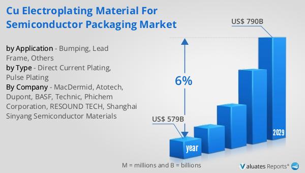
The outlook for the Global Cu Electroplating Material for Semiconductor Packaging Market is closely tied to the broader semiconductor industry, which was valued at approximately $579 billion in 2022. This market is projected to grow to $790 billion by 2029, reflecting a compound annual growth rate (CAGR) of 6% over the forecast period. This growth is driven by several factors, including the increasing demand for consumer electronics, automotive electronics, and other applications that rely on advanced semiconductor technologies. As the semiconductor industry continues to expand, the need for efficient and reliable packaging solutions becomes more critical, driving the demand for copper electroplating materials. The use of copper in semiconductor packaging offers several advantages, including excellent electrical conductivity, thermal performance, and mechanical strength, making it an ideal choice for various packaging applications. Additionally, the ongoing trend towards miniaturization and increased integration density in semiconductor devices further fuels the demand for high-performance packaging materials like copper. As a result, the Global Cu Electroplating Material for Semiconductor Packaging Market is expected to experience significant growth in the coming years, supported by the continued advancements in semiconductor technology and the increasing complexity of electronic devices. Overall, the market outlook for copper electroplating materials in semiconductor packaging is positive, with strong growth prospects driven by the evolving needs of the semiconductor industry.
| Report Metric | Details |
| Report Name | Cu Electroplating Material for Semiconductor Packaging Market |
| Accounted market size in year | US$ 579 billion |
| Forecasted market size in 2029 | US$ 790 billion |
| CAGR | 6% |
| Base Year | year |
| Forecasted years | 2025 - 2029 |
| by Type |
|
| by Application |
|
| Production by Region |
|
| Consumption by Region |
|
| By Company | MacDermid, Atotech, Dupont, BASF, Technic, Phichem Corporation, RESOUND TECH, Shanghai Sinyang Semiconductor Materials |
| Forecast units | USD million in value |
| Report coverage | Revenue and volume forecast, company share, competitive landscape, growth factors and trends |


