What is Global Tin Plating Solution for Semiconductor Packaging Market?
The Global Tin Plating Solution for Semiconductor Packaging Market is a specialized segment within the broader semiconductor industry, focusing on the application of tin plating in semiconductor packaging. Tin plating is a crucial process that involves coating semiconductor components with a thin layer of tin to enhance their performance and longevity. This process is essential for protecting semiconductor devices from corrosion, improving solderability, and ensuring reliable electrical connections. The market for tin plating solutions is driven by the increasing demand for semiconductors in various applications, including consumer electronics, automotive, and industrial sectors. As technology advances, the need for more efficient and reliable semiconductor packaging solutions grows, making tin plating an indispensable part of the manufacturing process. The market is characterized by continuous innovation and development of new plating techniques to meet the evolving needs of the semiconductor industry. Companies operating in this market are focused on providing high-quality, cost-effective tin plating solutions that comply with environmental regulations and industry standards. The global tin plating solution market is poised for growth as the demand for semiconductors continues to rise, driven by technological advancements and the proliferation of electronic devices.
Pure Tin, Tin Silver, Tin Lead in the Global Tin Plating Solution for Semiconductor Packaging Market:
In the Global Tin Plating Solution for Semiconductor Packaging Market, three primary types of tin plating are commonly used: Pure Tin, Tin Silver, and Tin Lead. Each of these has distinct properties and applications, catering to different needs within the semiconductor industry. Pure Tin plating is widely used due to its excellent solderability and corrosion resistance. It provides a reliable surface for soldering, which is crucial in semiconductor packaging. Pure Tin is also favored for its environmental friendliness, as it does not contain lead, making it compliant with RoHS (Restriction of Hazardous Substances) regulations. However, one of the challenges with Pure Tin is the potential for tin whisker growth, which can lead to short circuits. To mitigate this, manufacturers often employ additional processes or coatings to prevent whisker formation. Tin Silver plating, on the other hand, is known for its superior mechanical properties and thermal stability. The addition of silver enhances the plating's resistance to wear and improves its conductivity, making it suitable for high-performance applications. Tin Silver is often used in environments where components are subjected to high temperatures and mechanical stress. It also offers better resistance to tin whisker growth compared to Pure Tin, making it a preferred choice for critical applications. Tin Lead plating has been a traditional choice in the semiconductor industry due to its excellent solderability and resistance to whisker growth. The presence of lead in the alloy helps prevent the formation of tin whiskers, ensuring long-term reliability of the components. However, due to environmental concerns and regulatory restrictions, the use of Tin Lead plating has declined in recent years. Many manufacturers are transitioning to lead-free alternatives like Pure Tin and Tin Silver to comply with environmental regulations. Despite this, Tin Lead plating is still used in certain applications where its unique properties are required, and exemptions from regulations are granted. Each type of tin plating offers distinct advantages and challenges, and the choice of plating depends on the specific requirements of the semiconductor application. Manufacturers must carefully consider factors such as solderability, environmental impact, mechanical properties, and regulatory compliance when selecting a tin plating solution for semiconductor packaging.
Bumping, UBM, Wafer Level Packaging, Others in the Global Tin Plating Solution for Semiconductor Packaging Market:
The Global Tin Plating Solution for Semiconductor Packaging Market finds its application in several key areas, including Bumping, Under Bump Metallization (UBM), Wafer Level Packaging, and others. In the context of Bumping, tin plating is used to create small bumps on the surface of semiconductor wafers. These bumps serve as interconnects that facilitate the connection between the semiconductor die and the substrate or printed circuit board (PCB). Tin plating in bumping provides excellent solderability and ensures reliable electrical connections, which are critical for the performance of semiconductor devices. The use of tin plating in bumping is particularly important in flip-chip technology, where the die is mounted face-down on the substrate, requiring robust and reliable interconnects. Under Bump Metallization (UBM) is another area where tin plating plays a crucial role. UBM is a process that involves depositing a metal layer on the semiconductor wafer to enhance the adhesion and solderability of the bumps. Tin plating is often used in UBM to provide a solderable surface that ensures strong and reliable connections between the die and the substrate. The choice of tin plating in UBM depends on factors such as the type of solder used, the operating environment, and the specific requirements of the semiconductor application. Wafer Level Packaging (WLP) is an advanced packaging technology that involves packaging the semiconductor die at the wafer level, before it is diced into individual chips. Tin plating is used in WLP to provide a protective coating that enhances the solderability and reliability of the package. The use of tin plating in WLP helps improve the electrical performance of the package and ensures long-term reliability in various operating conditions. Other applications of tin plating in the semiconductor packaging market include lead frame plating, connector plating, and terminal plating. In these applications, tin plating provides corrosion resistance, enhances solderability, and ensures reliable electrical connections. The versatility and effectiveness of tin plating make it an essential component in the semiconductor packaging process, catering to a wide range of applications and requirements.
Global Tin Plating Solution for Semiconductor Packaging Market Outlook:
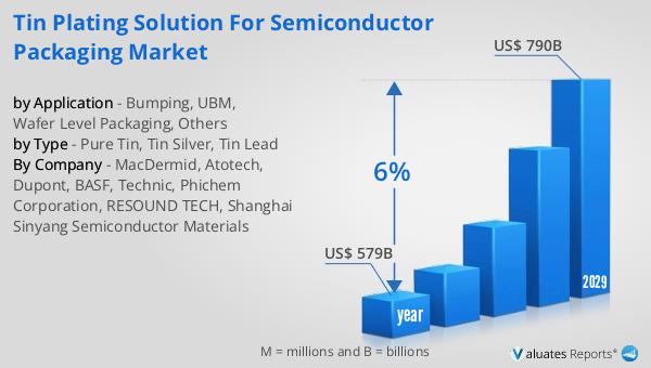
The outlook for the Global Tin Plating Solution for Semiconductor Packaging Market is closely tied to the overall growth of the semiconductor industry. In 2022, the global semiconductor market was valued at approximately US$ 579 billion. This market is projected to grow significantly, reaching an estimated value of US$ 790 billion by 2029. This growth represents a compound annual growth rate (CAGR) of 6% over the forecast period. The increasing demand for semiconductors in various applications, including consumer electronics, automotive, and industrial sectors, is a key driver of this growth. As technology continues to advance, the need for more efficient and reliable semiconductor packaging solutions becomes increasingly important. Tin plating solutions play a crucial role in enhancing the performance and longevity of semiconductor devices, making them an integral part of the manufacturing process. The market for tin plating solutions is expected to benefit from the overall growth of the semiconductor industry, as manufacturers seek high-quality, cost-effective solutions that comply with environmental regulations and industry standards. The continuous innovation and development of new plating techniques will further drive the growth of the tin plating solution market, ensuring its relevance and importance in the semiconductor industry.
| Report Metric | Details |
| Report Name | Tin Plating Solution for Semiconductor Packaging Market |
| Accounted market size in year | US$ 579 billion |
| Forecasted market size in 2029 | US$ 790 billion |
| CAGR | 6% |
| Base Year | year |
| Forecasted years | 2025 - 2029 |
| by Type |
|
| by Application |
|
| Production by Region |
|
| Consumption by Region |
|
| By Company | MacDermid, Atotech, Dupont, BASF, Technic, Phichem Corporation, RESOUND TECH, Shanghai Sinyang Semiconductor Materials |
| Forecast units | USD million in value |
| Report coverage | Revenue and volume forecast, company share, competitive landscape, growth factors and trends |


