What is Global Copper Pillar Bump (CPB) Market?
The Global Copper Pillar Bump (CPB) Market is a significant segment within the semiconductor industry, focusing on the use of copper pillar bumps in integrated circuits and electronic devices. Copper pillar bumps are tiny, cylindrical structures made of copper that serve as interconnects between different layers of a semiconductor device. They are crucial in ensuring efficient electrical connections and enhancing the performance of electronic components. The market for CPB is driven by the increasing demand for miniaturized and high-performance electronic devices, such as smartphones, tablets, and wearable technology. As these devices become more compact and require greater functionality, the need for reliable and efficient interconnect solutions like copper pillar bumps grows. Additionally, the shift towards advanced packaging technologies, such as 3D packaging and system-in-package (SiP), further propels the demand for CPB. These technologies require robust interconnect solutions to accommodate the complex architectures and high-density integration of modern electronic devices. The global CPB market is characterized by continuous innovation and development, with manufacturers focusing on improving the reliability, performance, and cost-effectiveness of copper pillar bump solutions to meet the evolving needs of the electronics industry.
in the Global Copper Pillar Bump (CPB) Market:
In the Global Copper Pillar Bump (CPB) Market, various types of copper pillar bumps are utilized by customers based on their specific requirements and applications. One of the primary types is the standard copper pillar bump, which is widely used in general semiconductor applications. These bumps are typically cylindrical in shape and are designed to provide reliable electrical connections between different layers of a semiconductor device. They are favored for their excellent conductivity and mechanical strength, making them suitable for a wide range of electronic devices. Another type is the micro copper pillar bump, which is smaller in size and used in applications where space is a critical factor. These micro bumps are essential in advanced packaging technologies, such as 3D packaging and system-in-package (SiP), where high-density integration and miniaturization are required. The micro copper pillar bumps enable efficient interconnects in compact electronic devices, ensuring optimal performance and functionality. Additionally, there are customized copper pillar bumps that are tailored to meet specific customer needs. These customized solutions are designed to address unique challenges in particular applications, such as high-frequency or high-power devices. Manufacturers work closely with customers to develop copper pillar bumps that meet their specific requirements, ensuring optimal performance and reliability. Furthermore, the market also sees the use of copper pillar bumps with different plating materials, such as nickel or gold, to enhance their performance in specific applications. These plated copper pillar bumps offer improved corrosion resistance and better solderability, making them suitable for harsh environments or applications requiring high reliability. The choice of copper pillar bump type depends on various factors, including the application, device architecture, and performance requirements. Customers in the semiconductor industry carefully evaluate these factors to select the most appropriate copper pillar bump solution for their needs. As the demand for advanced electronic devices continues to grow, the Global Copper Pillar Bump Market is expected to see further diversification in the types of copper pillar bumps available, with manufacturers focusing on developing innovative solutions to meet the evolving needs of their customers.
in the Global Copper Pillar Bump (CPB) Market:
The Global Copper Pillar Bump (CPB) Market finds applications across a wide range of industries, driven by the need for efficient and reliable interconnect solutions in electronic devices. One of the primary applications of copper pillar bumps is in the semiconductor industry, where they are used in the fabrication of integrated circuits (ICs). Copper pillar bumps serve as critical interconnects between different layers of an IC, ensuring efficient electrical connections and enhancing the overall performance of the device. They are particularly important in advanced packaging technologies, such as 3D packaging and system-in-package (SiP), where high-density integration and miniaturization are essential. In addition to the semiconductor industry, copper pillar bumps are also used in consumer electronics, such as smartphones, tablets, and wearable devices. These devices require compact and high-performance components, and copper pillar bumps provide the necessary interconnect solutions to meet these demands. The use of copper pillar bumps in consumer electronics ensures reliable performance and functionality, contributing to the overall user experience. Furthermore, the automotive industry is another significant application area for copper pillar bumps. With the increasing integration of electronic components in vehicles, such as advanced driver-assistance systems (ADAS) and infotainment systems, the demand for reliable interconnect solutions is growing. Copper pillar bumps offer the necessary performance and reliability to support the complex electronic architectures in modern vehicles. Additionally, the telecommunications industry also utilizes copper pillar bumps in the development of high-frequency and high-speed communication devices. These devices require efficient interconnect solutions to ensure optimal signal transmission and performance. Copper pillar bumps provide the necessary electrical connections to support the high-frequency operations of these devices, making them an essential component in the telecommunications industry. Overall, the Global Copper Pillar Bump Market plays a crucial role in various applications, providing reliable and efficient interconnect solutions to meet the demands of modern electronic devices across different industries.
Global Copper Pillar Bump (CPB) Market Outlook:
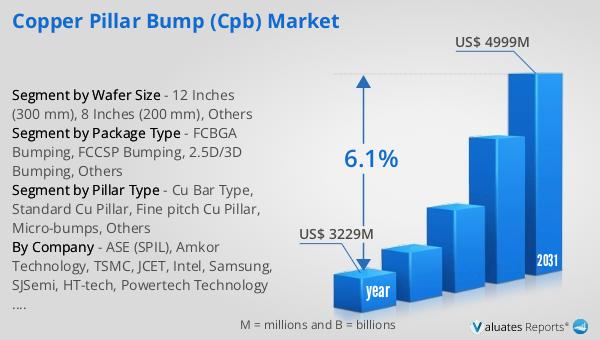
The global market for Copper Pillar Bump (CPB) was valued at approximately $3.229 billion in 2024 and is anticipated to expand to a revised size of around $4.999 billion by 2031. This growth is expected to occur at a compound annual growth rate (CAGR) of 6.1% over the forecast period. The market is dominated by the top ten players, who collectively hold over 83% of the global market share. This indicates a highly competitive landscape where a few key players have significant influence over market trends and developments. The growth in the CPB market is driven by the increasing demand for advanced electronic devices that require efficient and reliable interconnect solutions. As technology continues to evolve, the need for miniaturized and high-performance components becomes more critical, further propelling the demand for copper pillar bumps. The market's expansion is also supported by the ongoing advancements in semiconductor packaging technologies, which require robust interconnect solutions to accommodate complex device architectures. As a result, manufacturers are focusing on innovation and development to enhance the performance and reliability of copper pillar bump solutions, ensuring they meet the evolving needs of the electronics industry. The dominance of the top players in the market highlights the importance of strategic partnerships and collaborations to maintain a competitive edge and drive growth in the Global Copper Pillar Bump Market.
| Report Metric | Details |
| Report Name | Copper Pillar Bump (CPB) Market |
| Accounted market size in year | US$ 3229 million |
| Forecasted market size in 2031 | US$ 4999 million |
| CAGR | 6.1% |
| Base Year | year |
| Forecasted years | 2025 - 2031 |
| Segment by Pillar Type |
|
| Segment by Package Type |
|
| Segment by Wafer Size |
|
| Production by Region |
|
| Consumption by Region |
|
| By Company | ASE (SPIL), Amkor Technology, TSMC, JCET, Intel, Samsung, SJSemi, HT-tech, Powertech Technology Inc. (PTI), Tongfu Microelectronics (TFME), Nepes, LB Semicon Inc, SFA Semicon, International Micro Industries, Inc. (IMI), Raytek Semiconductor, Winstek Semiconductor, Hana Micron, ChipMOS TECHNOLOGIES, Chipbond Technology Corporation, Hefei Chipmore Technology, Ningbo ChipEx Semiconductor Co., Ltd, UTAC |
| Forecast units | USD million in value |
| Report coverage | Revenue and volume forecast, company share, competitive landscape, growth factors and trends |


