What is Global Electron Beam Defect Review Equipment Market?
The Global Electron Beam Defect Review Equipment Market is a specialized segment within the semiconductor industry that focuses on the use of electron beam technology to identify and analyze defects in semiconductor wafers. This equipment is crucial for ensuring the quality and reliability of semiconductor devices, which are integral to a wide range of electronic products. Electron beam defect review equipment uses a focused beam of electrons to scan the surface of a wafer, allowing for high-resolution imaging and precise defect detection. This technology is particularly valuable in the production of advanced semiconductor nodes, where the complexity and density of circuits make defect detection challenging. The market for this equipment is driven by the increasing demand for smaller, more powerful, and energy-efficient electronic devices, which require advanced semiconductor manufacturing processes. As technology continues to evolve, the need for sophisticated defect review equipment is expected to grow, supporting the development of next-generation electronic products. The market is characterized by continuous innovation, with manufacturers striving to enhance the capabilities of their equipment to meet the stringent requirements of modern semiconductor fabrication. This dynamic market plays a critical role in the advancement of the semiconductor industry, enabling the production of high-quality, reliable electronic components.
5-7nm Process, 10-16nm Process, 20-28nm Process, Others in the Global Electron Beam Defect Review Equipment Market:
The Global Electron Beam Defect Review Equipment Market is intricately linked to various semiconductor manufacturing processes, including the 5-7nm, 10-16nm, and 20-28nm processes, among others. Each of these processes represents a different level of technological advancement in semiconductor fabrication, with smaller nanometer processes indicating more advanced technology. The 5-7nm process is at the cutting edge of semiconductor manufacturing, allowing for the production of highly efficient and powerful chips. This process requires extremely precise defect detection capabilities, as even the smallest defect can significantly impact the performance of the final product. Electron beam defect review equipment is essential in this context, providing the high-resolution imaging necessary to identify and analyze defects at such a small scale. The 10-16nm process, while slightly less advanced than the 5-7nm process, still demands a high level of precision in defect detection. This process is commonly used in the production of high-performance computing devices and advanced consumer electronics. Electron beam defect review equipment plays a crucial role in ensuring the quality and reliability of chips produced using this process, helping manufacturers maintain competitive advantage in the market. The 20-28nm process represents a more mature technology, often used in the production of a wide range of electronic devices, from smartphones to automotive electronics. While the defect detection requirements for this process are not as stringent as those for smaller nanometer processes, electron beam defect review equipment is still vital for maintaining product quality and reducing manufacturing costs. By identifying defects early in the production process, manufacturers can minimize waste and improve yield, ultimately enhancing profitability. Beyond these specific processes, the Global Electron Beam Defect Review Equipment Market also serves other semiconductor manufacturing needs. As the industry continues to evolve, new processes and technologies are constantly being developed, each with its own unique defect detection challenges. Electron beam defect review equipment manufacturers must continuously innovate to keep pace with these changes, developing new solutions that meet the evolving needs of the semiconductor industry. This ongoing innovation is a key driver of growth in the market, as manufacturers seek to enhance the capabilities of their equipment to support the production of next-generation semiconductor devices. Overall, the Global Electron Beam Defect Review Equipment Market is a dynamic and rapidly evolving segment of the semiconductor industry, playing a critical role in the advancement of semiconductor manufacturing technology.
200mm Wafer, 300mm Wafer, Mask, Others in the Global Electron Beam Defect Review Equipment Market:
The Global Electron Beam Defect Review Equipment Market finds extensive application in various areas of semiconductor manufacturing, including 200mm wafers, 300mm wafers, masks, and other related components. Each of these areas presents unique challenges and opportunities for defect detection, requiring specialized equipment and techniques to ensure the highest levels of quality and reliability. In the context of 200mm wafers, electron beam defect review equipment is used to identify and analyze defects that can impact the performance and yield of semiconductor devices. These wafers are commonly used in the production of a wide range of electronic components, from consumer electronics to industrial applications. The ability to detect and address defects early in the manufacturing process is crucial for maintaining product quality and reducing production costs. Electron beam technology provides the high-resolution imaging necessary to identify even the smallest defects, helping manufacturers optimize their production processes and improve yield. The use of electron beam defect review equipment is even more critical in the production of 300mm wafers, which are used in the fabrication of advanced semiconductor devices. These larger wafers allow for the production of more chips per wafer, increasing efficiency and reducing costs. However, the increased complexity and density of circuits on these wafers also make defect detection more challenging. Electron beam technology is essential for identifying and analyzing defects at this scale, providing the precision and accuracy needed to ensure the quality and reliability of the final product. Masks, which are used in the photolithography process to transfer circuit patterns onto semiconductor wafers, also benefit from the use of electron beam defect review equipment. Defects in masks can lead to significant issues in the final product, making defect detection and analysis a critical part of the manufacturing process. Electron beam technology provides the high-resolution imaging necessary to identify defects in masks, helping manufacturers maintain the integrity of their production processes and ensure the quality of their products. Beyond these specific areas, the Global Electron Beam Defect Review Equipment Market also serves other components and processes within the semiconductor industry. As technology continues to advance, new applications and challenges are constantly emerging, requiring ongoing innovation and development in defect detection technology. Manufacturers of electron beam defect review equipment must continuously adapt to these changes, developing new solutions that meet the evolving needs of the industry. This ongoing innovation is a key driver of growth in the market, as manufacturers seek to enhance the capabilities of their equipment to support the production of next-generation semiconductor devices. Overall, the Global Electron Beam Defect Review Equipment Market plays a critical role in ensuring the quality and reliability of semiconductor devices, supporting the advancement of technology and the development of new electronic products.
Global Electron Beam Defect Review Equipment Market Outlook:
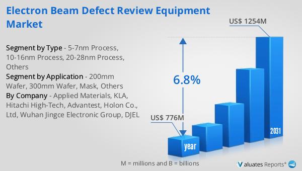
In 2024, the global market for Electron Beam Defect Review Equipment was valued at approximately $776 million. This market is anticipated to expand significantly, reaching an estimated value of $1,254 million by 2031. This growth trajectory represents a compound annual growth rate (CAGR) of 6.8% over the forecast period. The increasing demand for advanced semiconductor devices, driven by the proliferation of electronic products and the need for more efficient and powerful chips, is a key factor contributing to this market expansion. As semiconductor manufacturing processes become more complex, the need for precise and accurate defect detection becomes increasingly critical. Electron beam defect review equipment provides the high-resolution imaging necessary to identify and analyze defects in semiconductor wafers, masks, and other components, ensuring the quality and reliability of the final product. The market is characterized by continuous innovation, with manufacturers striving to enhance the capabilities of their equipment to meet the evolving needs of the semiconductor industry. This dynamic market plays a crucial role in the advancement of semiconductor technology, supporting the development of next-generation electronic products and driving growth in the global economy. As the market continues to evolve, manufacturers of electron beam defect review equipment must remain agile and responsive to changing industry demands, developing new solutions that address the unique challenges of modern semiconductor fabrication.
| Report Metric | Details |
| Report Name | Electron Beam Defect Review Equipment Market |
| Accounted market size in year | US$ 776 million |
| Forecasted market size in 2031 | US$ 1254 million |
| CAGR | 6.8% |
| Base Year | year |
| Forecasted years | 2025 - 2031 |
| Segment by Type |
|
| Segment by Application |
|
| Production by Region |
|
| Consumption by Region |
|
| By Company | Applied Materials, KLA, Hitachi High-Tech, Advantest, Holon Co., Ltd, Wuhan Jingce Electronic Group, DJEL |
| Forecast units | USD million in value |
| Report coverage | Revenue and volume forecast, company share, competitive landscape, growth factors and trends |


