What is Global E-Beam Wafer Defect Inspection Systems Market?
The Global E-Beam Wafer Defect Inspection Systems Market is a specialized segment within the semiconductor industry that focuses on the detection and analysis of defects in semiconductor wafers using electron beam technology. These systems are crucial for ensuring the quality and reliability of semiconductor devices, which are integral to a wide range of electronic products. As the demand for smaller, more powerful, and energy-efficient electronic devices continues to grow, the need for advanced inspection systems that can detect even the smallest defects becomes increasingly important. E-Beam Wafer Defect Inspection Systems utilize electron beams to scan the surface of semiconductor wafers, identifying defects that could potentially impact the performance and yield of semiconductor devices. This market is driven by the continuous advancements in semiconductor technology, the increasing complexity of semiconductor devices, and the need for high precision in defect detection. The systems are used by semiconductor manufacturers to improve production efficiency, reduce costs, and ensure the delivery of high-quality products to the market. As the semiconductor industry continues to evolve, the Global E-Beam Wafer Defect Inspection Systems Market is expected to play a critical role in supporting the development and production of next-generation electronic devices.
EBI, DR-SEM in the Global E-Beam Wafer Defect Inspection Systems Market:
E-Beam Inspection (EBI) and Defect Review Scanning Electron Microscopy (DR-SEM) are two pivotal technologies within the Global E-Beam Wafer Defect Inspection Systems Market, each serving distinct yet complementary roles in the semiconductor manufacturing process. EBI is primarily used for the rapid scanning and identification of defects on semiconductor wafers. It employs a focused electron beam to scan the wafer surface, detecting anomalies that could affect the performance of the final semiconductor device. The high resolution of EBI systems allows for the detection of very small defects, which is crucial as semiconductor devices become increasingly miniaturized. EBI systems are typically used in the early stages of the manufacturing process to ensure that wafers meet the required quality standards before further processing. On the other hand, DR-SEM is used for a more detailed analysis of defects identified by EBI systems. Once a defect is detected, DR-SEM provides a high-resolution image of the defect, allowing engineers to understand its nature and potential impact on device performance. This detailed analysis is essential for determining the root cause of defects and implementing corrective actions to prevent their recurrence. DR-SEM is particularly valuable in the research and development phase, where understanding the nature of defects can lead to improvements in manufacturing processes and the development of more robust semiconductor devices. Both EBI and DR-SEM are integral to the quality control process in semiconductor manufacturing, ensuring that only wafers that meet stringent quality standards proceed to the next stages of production. As semiconductor devices become more complex, the role of EBI and DR-SEM in defect detection and analysis becomes increasingly important. These technologies not only help in maintaining high yield rates but also contribute to the overall reliability and performance of semiconductor devices. The integration of EBI and DR-SEM into the manufacturing process allows semiconductor manufacturers to identify and address defects early, reducing the risk of costly rework and improving the overall efficiency of the production process. As the semiconductor industry continues to advance, the demand for EBI and DR-SEM technologies is expected to grow, driven by the need for more precise and efficient defect detection and analysis solutions.
200mm Wafer, 300mm Wafer, Others in the Global E-Beam Wafer Defect Inspection Systems Market:
The Global E-Beam Wafer Defect Inspection Systems Market finds significant application in the inspection of 200mm and 300mm wafers, as well as other wafer sizes, each presenting unique challenges and opportunities. The 200mm wafer, once the industry standard, is still widely used in the production of various semiconductor devices, particularly in mature markets and for specific applications such as analog devices and power semiconductors. E-Beam Wafer Defect Inspection Systems are crucial for maintaining the quality and yield of 200mm wafers, which are often produced in older fabrication facilities with established processes. These systems help identify defects that could impact device performance, allowing manufacturers to maintain high standards of quality and reliability. The 300mm wafer, on the other hand, represents the current standard for high-volume semiconductor manufacturing, particularly for advanced logic and memory devices. The larger size of 300mm wafers allows for more chips to be produced per wafer, improving production efficiency and reducing costs. However, the increased complexity of devices produced on 300mm wafers necessitates more advanced inspection solutions. E-Beam Wafer Defect Inspection Systems provide the high resolution and precision needed to detect defects on these larger wafers, ensuring that only wafers meeting the highest quality standards proceed to the next stages of production. In addition to 200mm and 300mm wafers, E-Beam Wafer Defect Inspection Systems are also used for other wafer sizes, including emerging sizes such as 450mm wafers. While 450mm wafers are not yet widely adopted, they represent the future of semiconductor manufacturing, offering the potential for even greater production efficiencies. As the industry moves towards larger wafer sizes, the demand for advanced inspection solutions capable of handling the increased complexity and precision requirements will continue to grow. E-Beam Wafer Defect Inspection Systems are well-positioned to meet these demands, providing the high-resolution imaging and defect detection capabilities needed to support the production of next-generation semiconductor devices. Overall, the Global E-Beam Wafer Defect Inspection Systems Market plays a critical role in ensuring the quality and reliability of semiconductor devices across a range of wafer sizes, supporting the continued growth and advancement of the semiconductor industry.
Global E-Beam Wafer Defect Inspection Systems Market Outlook:
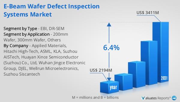
In 2024, the worldwide market for E-Beam Wafer Defect Inspection Systems was estimated to be worth approximately $2,194 million. This market is anticipated to expand significantly, reaching an adjusted valuation of around $3,411 million by 2031. This growth trajectory represents a compound annual growth rate (CAGR) of 6.4% over the forecast period. The increasing demand for advanced semiconductor devices, driven by technological advancements and the proliferation of electronic devices, is a key factor contributing to this market growth. As semiconductor devices become more complex and miniaturized, the need for precise and efficient defect inspection solutions becomes increasingly critical. E-Beam Wafer Defect Inspection Systems, with their high-resolution imaging and defect detection capabilities, are well-suited to meet these demands. The market's growth is also supported by the ongoing investments in semiconductor manufacturing facilities and the continuous development of new technologies and processes. As the semiconductor industry continues to evolve, the Global E-Beam Wafer Defect Inspection Systems Market is expected to play a vital role in supporting the production of high-quality, reliable semiconductor devices. This market outlook highlights the significant opportunities for growth and innovation within this specialized segment of the semiconductor industry.
| Report Metric | Details |
| Report Name | E-Beam Wafer Defect Inspection Systems Market |
| Accounted market size in year | US$ 2194 million |
| Forecasted market size in 2031 | US$ 3411 million |
| CAGR | 6.4% |
| Base Year | year |
| Forecasted years | 2025 - 2031 |
| Segment by Type |
|
| Segment by Application |
|
| Production by Region |
|
| Consumption by Region |
|
| By Company | Applied Materials, Hitachi High-Tech, ASML, KLA, Suzhou AISTech, Huayan Xince Semiconductor (Suzhou) Co., Ltd, Wuhan Jingce Electronic Group, DJEL, Wellrun Microelectronics, Suzhou Siscantech |
| Forecast units | USD million in value |
| Report coverage | Revenue and volume forecast, company share, competitive landscape, growth factors and trends |


