What is Global Electron Beam Inspection System Market?
The Global Electron Beam Inspection System Market is a specialized segment within the broader semiconductor inspection industry. This market focuses on the use of electron beam technology to inspect semiconductor wafers and masks, which are critical components in the manufacturing of integrated circuits. Electron beam inspection systems are highly valued for their ability to detect defects at a nanometer scale, providing a level of precision that is essential for the production of advanced semiconductor devices. These systems are particularly important as the semiconductor industry continues to push the boundaries of miniaturization and complexity. The market for these systems is driven by the increasing demand for high-performance electronic devices, which require ever-smaller and more complex semiconductor components. As a result, manufacturers are investing in advanced inspection technologies to ensure the quality and reliability of their products. The Global Electron Beam Inspection System Market is characterized by rapid technological advancements and a high level of competition among key players, who are constantly striving to develop more efficient and accurate inspection solutions. This market is expected to grow significantly in the coming years, driven by the ongoing evolution of the semiconductor industry and the increasing need for precise inspection capabilities.
EBI, DR-SEM in the Global Electron Beam Inspection System Market:
Electron Beam Inspection (EBI) and Defect Review Scanning Electron Microscopy (DR-SEM) are two critical technologies within the Global Electron Beam Inspection System Market. EBI systems utilize a focused beam of electrons to scan the surface of semiconductor wafers and masks, allowing for the detection of defects that are not visible using traditional optical inspection methods. This technology is particularly effective for identifying small defects, such as pattern deviations, particle contamination, and surface irregularities, which can significantly impact the performance and yield of semiconductor devices. EBI systems are equipped with advanced imaging capabilities, enabling them to capture high-resolution images of the inspected surfaces, which are then analyzed to identify and classify defects. This level of precision is essential for the production of next-generation semiconductor devices, which require extremely tight tolerances and high levels of reliability. DR-SEM, on the other hand, is a complementary technology that is used to review and analyze defects identified by EBI systems. It provides detailed information about the nature and origin of defects, allowing manufacturers to implement corrective actions and improve their production processes. DR-SEM systems are equipped with advanced imaging and analytical capabilities, enabling them to provide a comprehensive understanding of defect characteristics and their impact on device performance. Together, EBI and DR-SEM technologies play a crucial role in ensuring the quality and reliability of semiconductor devices, supporting the ongoing advancement of the semiconductor industry. The integration of these technologies into the manufacturing process allows for the early detection and correction of defects, reducing the risk of costly production errors and improving overall yield. As the demand for high-performance electronic devices continues to grow, the importance of EBI and DR-SEM technologies in the semiconductor manufacturing process is expected to increase, driving further innovation and development in the Global Electron Beam Inspection System Market.
Wafer, Mask in the Global Electron Beam Inspection System Market:
The Global Electron Beam Inspection System Market plays a vital role in the semiconductor manufacturing process, particularly in the inspection of wafers and masks. Wafers are thin slices of semiconductor material, such as silicon, that serve as the substrate for the fabrication of integrated circuits. The quality of these wafers is critical to the performance and reliability of the final semiconductor devices. Electron beam inspection systems are used to inspect wafers for defects that can occur during the manufacturing process, such as pattern deviations, particle contamination, and surface irregularities. These systems provide a high level of precision and accuracy, allowing manufacturers to detect and correct defects before they impact the performance of the final product. This is particularly important as the semiconductor industry continues to push the boundaries of miniaturization and complexity, requiring ever-smaller and more complex components. Masks, on the other hand, are used in the photolithography process to transfer circuit patterns onto the wafer surface. The quality of these masks is equally important, as any defects can be transferred to the wafer, resulting in faulty or suboptimal devices. Electron beam inspection systems are used to inspect masks for defects, ensuring that they meet the stringent quality standards required for semiconductor manufacturing. By providing detailed information about the nature and origin of defects, these systems enable manufacturers to implement corrective actions and improve their production processes. The use of electron beam inspection systems in the inspection of wafers and masks is essential for ensuring the quality and reliability of semiconductor devices, supporting the ongoing advancement of the semiconductor industry. As the demand for high-performance electronic devices continues to grow, the importance of these systems in the semiconductor manufacturing process is expected to increase, driving further innovation and development in the Global Electron Beam Inspection System Market.
Global Electron Beam Inspection System Market Outlook:
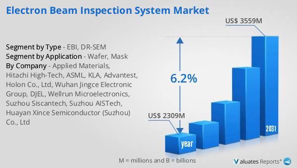
The global market for Electron Beam Inspection Systems was valued at approximately $2,309 million in 2024. This market is projected to expand significantly, reaching an estimated size of $3,559 million by 2031. This growth represents a compound annual growth rate (CAGR) of 6.2% over the forecast period. The expansion of this market is driven by the increasing demand for advanced semiconductor devices, which require precise and reliable inspection solutions. As the semiconductor industry continues to evolve, manufacturers are investing in cutting-edge inspection technologies to ensure the quality and performance of their products. Electron beam inspection systems are particularly valued for their ability to detect defects at a nanometer scale, providing a level of precision that is essential for the production of next-generation semiconductor devices. The market is characterized by rapid technological advancements and a high level of competition among key players, who are constantly striving to develop more efficient and accurate inspection solutions. As a result, the Global Electron Beam Inspection System Market is expected to experience significant growth in the coming years, driven by the ongoing evolution of the semiconductor industry and the increasing need for precise inspection capabilities.
| Report Metric | Details |
| Report Name | Electron Beam Inspection System Market |
| Accounted market size in year | US$ 2309 million |
| Forecasted market size in 2031 | US$ 3559 million |
| CAGR | 6.2% |
| Base Year | year |
| Forecasted years | 2025 - 2031 |
| Segment by Type |
|
| Segment by Application |
|
| Production by Region |
|
| Consumption by Region |
|
| By Company | Applied Materials, Hitachi High-Tech, ASML, KLA, Advantest, Holon Co., Ltd, Wuhan Jingce Electronic Group, DJEL, Wellrun Microelectronics, Suzhou Siscantech, Suzhou AISTech, Huayan Xince Semiconductor (Suzhou) Co., Ltd |
| Forecast units | USD million in value |
| Report coverage | Revenue and volume forecast, company share, competitive landscape, growth factors and trends |


