Friday, August 15, 2025

Global Wafer CMP Retainer Rings Market Research Report 2025

What is Global Wafer CMP Retainer Rings Market?

The Global Wafer CMP Retainer Rings Market is a specialized segment within the semiconductor industry, focusing on the components used in the chemical mechanical planarization (CMP) process. CMP is a critical step in semiconductor manufacturing, where it is used to smooth and flatten the wafer surface, ensuring that subsequent layers are applied evenly. Retainer rings play a crucial role in this process by holding the wafer in place during polishing, preventing slippage, and ensuring uniform pressure distribution. These rings are typically made from high-performance materials that can withstand the rigorous conditions of the CMP process, such as high temperatures and abrasive environments. The market for these retainer rings is driven by the increasing demand for semiconductors across various industries, including consumer electronics, automotive, and telecommunications. As technology advances, the need for more precise and efficient manufacturing processes grows, further fueling the demand for high-quality CMP retainer rings. The market is characterized by continuous innovation, with manufacturers striving to develop rings that offer improved durability, performance, and compatibility with various wafer sizes and materials. This market's growth is closely tied to the overall health of the semiconductor industry, making it a vital component of the global technology landscape.

Wafer CMP Retainer Rings Market

Polyphenylene Sulfide (PPS), Polyetheretherketone (PEEK), Polyethylene Terephthalate (PET), Others in the Global Wafer CMP Retainer Rings Market:

Polyphenylene Sulfide (PPS), Polyetheretherketone (PEEK), and Polyethylene Terephthalate (PET) are among the key materials used in the manufacturing of CMP retainer rings, each offering unique properties that make them suitable for different applications within the Global Wafer CMP Retainer Rings Market. PPS is a high-performance thermoplastic known for its exceptional chemical resistance, dimensional stability, and ability to withstand high temperatures. These properties make PPS an ideal choice for CMP retainer rings, as it can endure the harsh conditions of the CMP process without degrading. PPS rings are often used in applications where chemical exposure is a concern, providing reliable performance and longevity. PEEK, on the other hand, is renowned for its outstanding mechanical properties, including high strength, stiffness, and resistance to wear and fatigue. This makes PEEK an excellent material for retainer rings that require superior durability and performance under mechanical stress. PEEK rings are particularly favored in high-precision applications where maintaining tight tolerances is critical. PET, a more cost-effective option, offers good chemical resistance and mechanical properties, making it suitable for less demanding applications. While PET may not match the performance of PPS or PEEK in extreme conditions, it provides a viable alternative for applications where cost is a primary consideration. In addition to these materials, other advanced polymers and composites are also used in the production of CMP retainer rings, each selected based on the specific requirements of the application. The choice of material is influenced by factors such as the type of wafer being processed, the specific CMP process parameters, and the desired balance between performance and cost. As the semiconductor industry continues to evolve, the demand for materials that can meet the increasingly stringent requirements of CMP processes is expected to grow, driving further innovation and development in the Global Wafer CMP Retainer Rings Market.

300 mm Wafer, 200 mm Wafer, Others in the Global Wafer CMP Retainer Rings Market:

The usage of Global Wafer CMP Retainer Rings Market in different wafer sizes, such as 300 mm and 200 mm wafers, as well as other sizes, highlights the versatility and adaptability of these components in semiconductor manufacturing. The 300 mm wafer, being the largest standard size used in the industry, requires retainer rings that can accommodate its dimensions while ensuring precise and uniform polishing. The larger surface area of 300 mm wafers means that any imperfections during the CMP process can have a more significant impact on the final product, making the role of retainer rings even more critical. These rings must provide consistent pressure distribution and prevent any slippage or misalignment during polishing, ensuring that the wafer surface is perfectly planar. The demand for 300 mm wafers is driven by the need for higher production efficiency and cost-effectiveness, as larger wafers allow for more chips to be produced per batch. In contrast, 200 mm wafers, while smaller, still play a vital role in the semiconductor industry, particularly in the production of specialized and legacy devices. Retainer rings for 200 mm wafers must be designed to offer the same level of precision and reliability as those used for larger wafers, albeit on a smaller scale. The continued use of 200 mm wafers in certain applications underscores the importance of having a diverse range of retainer rings that can cater to different wafer sizes and manufacturing needs. Beyond the standard 300 mm and 200 mm wafers, the Global Wafer CMP Retainer Rings Market also addresses the requirements of other wafer sizes, which may be used in niche or emerging applications. These include smaller wafers used in research and development or specialized manufacturing processes, where the focus may be on innovation and experimentation rather than mass production. The ability to provide retainer rings for a wide range of wafer sizes demonstrates the market's commitment to supporting the diverse needs of the semiconductor industry. As technology continues to advance and new applications for semiconductors emerge, the demand for CMP retainer rings that can accommodate various wafer sizes and process requirements is expected to grow, further solidifying their role as an essential component in semiconductor manufacturing.

Global Wafer CMP Retainer Rings Market Outlook:

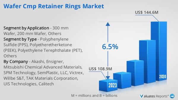
In 2024, the global market for Wafer CMP Retainer Rings was valued at approximately US$ 105 million, with projections indicating a growth to around US$ 162 million by 2031, reflecting a compound annual growth rate (CAGR) of 6.5% over the forecast period. Despite this overall growth, the largest regional market, Asia Pacific, experienced a decline of 2.0%. In contrast, the Americas saw a significant increase in sales, reaching US$ 142.1 billion, which marked a 17.0% year-on-year growth. Similarly, Europe and Japan also experienced positive growth, with sales in Europe reaching US$ 53.8 billion, up 12.6% year-on-year, and sales in Japan totaling US$ 48.1 billion, reflecting a 10.0% year-on-year increase. However, the Asia Pacific region, despite being the largest market, saw a decline in sales, totaling US$ 336.2 billion, down 2.0% year-on-year. This mixed performance across different regions highlights the varying dynamics and challenges faced by the Global Wafer CMP Retainer Rings Market. Factors such as regional economic conditions, technological advancements, and shifts in semiconductor manufacturing trends all play a role in influencing market performance. As the industry continues to evolve, understanding these regional differences will be crucial for stakeholders looking to navigate the complexities of the global market.


Report Metric Details
Report Name Wafer CMP Retainer Rings Market
Accounted market size in year US$ 105 million
Forecasted market size in 2031 US$ 162 million
CAGR 6.5%
Base Year year
Forecasted years 2025 - 2031
by Type
  • Polyphenylene Sulfide (PPS)
  • Polyetheretherketone (PEEK)
  • Polyethylene Terephthalate (PET)
  • Others
by Application
  • 300 mm Wafer
  • 200 mm Wafer
  • Others
Production by Region
  • North America
  • Europe
  • China
  • Japan
  • Taiwan
Consumption by Region
  • North America (United States, Canada)
  • Europe (Germany, France, UK, Italy, Russia)
  • Asia-Pacific (China, Japan, South Korea, Taiwan)
  • Southeast Asia (India)
  • Latin America (Mexico, Brazil)
By Company Akashi, Ensigner, Mitsubishi Chemical Advanced Materials, SPM Technology, SemPlastic, LLC, Victrex, Willbe S&T, TAK Materials Corporation, UIS Technologies, Calitech
Forecast units USD million in value
Report coverage Revenue and volume forecast, company share, competitive landscape, growth factors and trends

Global Semiconductor Lithography Machines Market Research Report 2025

What is Global Semiconductor Lithography Machines Market?

The Global Semiconductor Lithography Machines Market is a crucial segment of the semiconductor industry, focusing on the production of lithography machines used in the manufacturing of semiconductor devices. These machines are essential for creating the intricate patterns on silicon wafers that form the basis of integrated circuits. As the demand for smaller, more powerful, and energy-efficient electronic devices grows, the need for advanced lithography machines has increased. The market encompasses various types of lithography technologies, each catering to different manufacturing needs and technological advancements. The growth of this market is driven by the continuous evolution of semiconductor technology, which requires more precise and efficient lithography solutions. Companies in this market are investing heavily in research and development to innovate and improve the capabilities of their machines, ensuring they can meet the ever-increasing demands of the semiconductor industry. The market is characterized by a few dominant players who hold significant market shares, reflecting the high level of expertise and technological advancement required in this field. As the semiconductor industry continues to expand, the Global Semiconductor Lithography Machines Market is expected to play a pivotal role in shaping the future of electronics manufacturing.

Semiconductor Lithography Machines Market

EUV Lithography System, ArFi Lithography System, ArF dry Lithography System, KrF Lithography System, I-line Lithography System in the Global Semiconductor Lithography Machines Market:

EUV (Extreme Ultraviolet) Lithography Systems represent the cutting-edge technology in the Global Semiconductor Lithography Machines Market. These systems use extremely short wavelengths of light to create very fine patterns on semiconductor wafers, enabling the production of smaller and more powerful chips. EUV lithography is essential for manufacturing the latest generation of semiconductors, which require incredibly precise patterning to function effectively. ArFi (Argon Fluoride Immersion) Lithography Systems are another advanced technology used in the semiconductor industry. These systems use a combination of argon fluoride lasers and immersion techniques to achieve high-resolution patterning. ArFi lithography is particularly useful for producing chips with smaller nodes, which are crucial for modern electronic devices. ArF Dry Lithography Systems, on the other hand, do not use immersion techniques but still rely on argon fluoride lasers to create patterns on wafers. These systems are typically used for less demanding applications where extreme precision is not as critical. KrF (Krypton Fluoride) Lithography Systems utilize krypton fluoride lasers to produce patterns on semiconductor wafers. While not as advanced as EUV or ArFi systems, KrF lithography is still widely used for many applications due to its reliability and cost-effectiveness. I-line Lithography Systems are one of the older technologies in the market, using ultraviolet light to create patterns on wafers. Despite being less advanced than newer technologies, I-line systems are still in use for certain applications where high precision is not required. Each of these lithography systems plays a vital role in the semiconductor manufacturing process, catering to different needs and technological requirements. The choice of system depends on various factors, including the desired resolution, cost considerations, and the specific application for which the semiconductor is being produced. As the semiconductor industry continues to evolve, the demand for these diverse lithography systems is expected to grow, driving further innovation and development in the Global Semiconductor Lithography Machines Market.

IDM, Foundry in the Global Semiconductor Lithography Machines Market:

In the realm of semiconductor manufacturing, the Global Semiconductor Lithography Machines Market finds significant application in Integrated Device Manufacturers (IDMs) and foundries. IDMs are companies that design, manufacture, and sell integrated circuit products. They rely heavily on advanced lithography machines to produce high-quality semiconductor devices. The precision and efficiency of these machines are crucial for IDMs, as they directly impact the performance and reliability of the final products. By utilizing state-of-the-art lithography systems, IDMs can achieve the high levels of accuracy and detail required for modern semiconductor devices. This capability is essential for maintaining competitiveness in the fast-paced electronics market, where innovation and performance are key drivers of success. Foundries, on the other hand, are companies that specialize in manufacturing semiconductor devices for other companies. They do not design their own products but instead focus on providing manufacturing services to other firms. For foundries, the ability to offer cutting-edge manufacturing capabilities is vital for attracting and retaining clients. Advanced lithography machines enable foundries to produce a wide range of semiconductor devices with varying levels of complexity and precision. This versatility is crucial for meeting the diverse needs of their clients, who may require different types of semiconductors for various applications. By investing in the latest lithography technologies, foundries can ensure they remain competitive in the global market, offering high-quality manufacturing services that meet the evolving demands of the semiconductor industry. Both IDMs and foundries play a critical role in the semiconductor supply chain, and their reliance on advanced lithography machines underscores the importance of the Global Semiconductor Lithography Machines Market. As the demand for more sophisticated and efficient semiconductor devices continues to grow, the need for cutting-edge lithography solutions will only increase, driving further advancements in this vital market segment.

Global Semiconductor Lithography Machines Market Outlook:

The worldwide market for Semiconductor Lithography Machines was valued at $27,060 million in 2024 and is anticipated to expand to a revised size of $41,670 million by 2031, reflecting a compound annual growth rate (CAGR) of 6.5% over the forecast period. ASML stands as the largest manufacturer, commanding over 90% of the market share, while Nikon and Canon each account for 5% of the market share. In the realm of KrF lithography machines, ASML, Nikon, and Canon dominate, with ASML holding more than 70% of the market share. The global semiconductor market was valued at $526.8 billion in 2023 and is projected to reach $780.7 billion by 2030. Our research indicates that the global semiconductor manufacturing wafer fabrication market is expected to grow from $251.7 billion in 2023 to $506.5 billion by 2030, at a CAGR of 40.49% during the forecast period. This growth underscores the critical role of semiconductor lithography machines in the broader semiconductor industry, as they are essential for producing the advanced chips that power modern electronic devices. The market's expansion reflects the increasing demand for more powerful and efficient semiconductors, driven by technological advancements and the growing need for high-performance electronics.


Report Metric Details
Report Name Semiconductor Lithography Machines Market
Accounted market size in year US$ 27060 million
Forecasted market size in 2031 US$ 41670 million
CAGR 6.5%
Base Year year
Forecasted years 2025 - 2031
by Type
  • EUV Lithography System
  • ArFi Lithography System
  • ArF dry Lithography System
  • KrF Lithography System
  • I-line Lithography System
by Application
  • IDM
  • Foundry
Production by Region
  • Netherlands
  • Japan
  • China
Consumption by Region
  • North America (United States, Canada)
  • Europe (Germany, France, UK, Italy, Russia)
  • Asia-Pacific (China, Japan, South Korea, Taiwan)
  • Southeast Asia (India)
  • Latin America (Mexico, Brazil)
By Company ASML, Nikon, Canon, Shanghai Micro Electronics Equipment
Forecast units USD million in value
Report coverage Revenue and volume forecast, company share, competitive landscape, growth factors and trends

Global Wafer Used CVD Equipment Market Research Report 2025

What is Global Wafer Used CVD Equipment Market?

The Global Wafer Used CVD Equipment Market is a specialized segment within the semiconductor industry that focuses on the equipment used for Chemical Vapor Deposition (CVD) processes on wafers. Wafers are thin slices of semiconductor material, such as silicon, used in the fabrication of integrated circuits and other microdevices. CVD is a critical process in semiconductor manufacturing, where a solid material is deposited from a vapor onto the wafer surface, forming thin films that are essential for creating electronic components. This market encompasses various types of CVD equipment, each designed to meet specific requirements of the semiconductor manufacturing process. The demand for CVD equipment is driven by the continuous advancement in semiconductor technology, which requires precise and efficient deposition techniques to produce smaller, faster, and more energy-efficient electronic devices. As the semiconductor industry continues to grow, fueled by the increasing demand for electronics in various sectors such as consumer electronics, automotive, and telecommunications, the Global Wafer Used CVD Equipment Market is expected to expand, offering opportunities for innovation and development in CVD technologies.

Wafer Used CVD Equipment Market

PECVD, LPCVD, ALD, Others in the Global Wafer Used CVD Equipment Market:

In the Global Wafer Used CVD Equipment Market, several types of CVD processes are utilized, each with its unique characteristics and applications. Plasma Enhanced Chemical Vapor Deposition (PECVD) is a widely used technique that employs plasma to enhance the chemical reaction rates of the precursors, allowing for lower deposition temperatures. This is particularly beneficial for depositing films on temperature-sensitive substrates, making PECVD ideal for applications in the production of dielectric layers and passivation films in semiconductor devices. PECVD is known for its ability to produce high-quality films with good uniformity and step coverage, which are crucial for the performance and reliability of electronic components.

IDM, Foundry in the Global Wafer Used CVD Equipment Market:

Low-Pressure Chemical Vapor Deposition (LPCVD) is another prominent method in the CVD equipment market. LPCVD operates at reduced pressures, which helps in achieving uniform film thickness over large wafer areas. This technique is commonly used for depositing polysilicon, silicon nitride, and silicon dioxide films. LPCVD is favored for its excellent film uniformity and high throughput, making it suitable for mass production environments. The low-pressure environment also reduces the risk of unwanted reactions, leading to high-purity films that are essential for advanced semiconductor applications.

Global Wafer Used CVD Equipment Market Outlook:

Atomic Layer Deposition (ALD) is a specialized form of CVD that allows for the deposition of ultra-thin films with atomic-level precision. ALD is characterized by its sequential, self-limiting surface reactions, which enable precise control over film thickness and composition. This makes ALD particularly valuable for applications requiring conformal coatings on complex 3D structures, such as in the fabrication of high-k dielectrics and metal gate stacks in advanced transistors. The ability to deposit films with atomic precision makes ALD a critical technology for the continued scaling of semiconductor devices.


Report Metric Details
Report Name Wafer Used CVD Equipment Market
Accounted market size in year US$ 9742 million
Forecasted market size in 2031 US$ 14690 million
CAGR 6.1%
Base Year year
Forecasted years 2025 - 2031
by Type
  • PECVD
  • LPCVD
  • ALD
  • Others
by Application
  • IDM
  • Foundry
Production by Region
  • North America
  • Europe
  • China
  • Japan
  • Korea
Consumption by Region
  • North America (United States, Canada)
  • Europe (Germany, France, UK, Italy, Russia)
  • Asia-Pacific (China, Japan, South Korea, Taiwan)
  • Southeast Asia (India)
  • Latin America (Mexico, Brazil)
By Company Applied Materials, Lam Research, Tokyo Electron, ASM International, Kokusai Electric, Wonik IPS, Eugene Technology, Jusung Engineering, TES, SPTS Technologies (KLA), Veeco, CVD Equipment, Piotech, NAURA Technology
Forecast units USD million in value
Report coverage Revenue and volume forecast, company share, competitive landscape, growth factors and trends

Global Perfluoroelastomer (FFKM) Seals and Parts for Semiconductor Market Research Report 2025

What is Global Perfluoroelastomer (FFKM) Seals and Parts for Semiconductor Market?

Global Perfluoroelastomer (FFKM) seals and parts are specialized components used in the semiconductor industry, known for their exceptional resistance to extreme temperatures and harsh chemical environments. These seals and parts are crafted from perfluoroelastomer, a type of synthetic rubber that combines the resilience of elastomers with the chemical resistance of fluoropolymers. This unique combination makes FFKM seals and parts indispensable in semiconductor manufacturing, where they are used to ensure the integrity and reliability of equipment and processes. The semiconductor industry demands materials that can withstand aggressive chemicals and high temperatures, and FFKM seals and parts meet these requirements with ease. They are used in various applications, including wafer processing, etching, and deposition, where maintaining a contaminant-free environment is crucial. The global market for these components is driven by the increasing demand for semiconductors in various industries, including electronics, automotive, and telecommunications. As technology advances and the need for smaller, more powerful devices grows, the demand for high-performance materials like FFKM seals and parts is expected to rise, making them a critical component in the semiconductor supply chain.

Perfluoroelastomer (FFKM) Seals and Parts for Semiconductor Market

O-Ring, Gasket, Others in the Global Perfluoroelastomer (FFKM) Seals and Parts for Semiconductor Market:

In the realm of Global Perfluoroelastomer (FFKM) Seals and Parts for the Semiconductor Market, components such as O-Rings, gaskets, and other specialized parts play a pivotal role. O-Rings, often considered the backbone of sealing solutions, are circular rings used to prevent the passage of liquids or gases. In the semiconductor industry, FFKM O-Rings are prized for their ability to withstand extreme temperatures and aggressive chemicals, ensuring that the delicate processes involved in semiconductor manufacturing remain uncontaminated. These O-Rings are used in various equipment, including pumps, valves, and reactors, where they provide a reliable seal that can endure the harsh conditions of semiconductor fabrication. Gaskets, on the other hand, are flat seals that fill the space between two or more mating surfaces, preventing leakage from or into the joined objects while under compression. FFKM gaskets are essential in semiconductor equipment, where they are used in applications such as chemical vapor deposition (CVD) and plasma etching. Their superior chemical resistance and thermal stability make them ideal for maintaining the integrity of semiconductor processes. Beyond O-Rings and gaskets, other FFKM parts, such as diaphragms, seals, and custom-molded components, are also crucial in the semiconductor industry. These parts are often used in critical applications where standard materials would fail, providing the necessary durability and performance to ensure the smooth operation of semiconductor manufacturing equipment. The demand for these components is driven by the need for high-performance materials that can withstand the rigorous demands of semiconductor production. As the semiconductor industry continues to evolve, the importance of FFKM seals and parts in ensuring the reliability and efficiency of manufacturing processes cannot be overstated. Their ability to maintain performance in extreme conditions makes them an indispensable component in the quest for smaller, faster, and more efficient semiconductor devices.

Wafer Suppliers, Semiconductor Equipment OEMs in the Global Perfluoroelastomer (FFKM) Seals and Parts for Semiconductor Market:

The usage of Global Perfluoroelastomer (FFKM) Seals and Parts in the semiconductor market is particularly significant among wafer suppliers and semiconductor equipment OEMs. Wafer suppliers rely on FFKM seals and parts to maintain the purity and integrity of their products. During the wafer fabrication process, maintaining a contaminant-free environment is crucial, as even the smallest impurity can lead to defects in the final semiconductor product. FFKM seals and parts provide the necessary chemical resistance and thermal stability to ensure that the wafer processing environment remains uncontaminated. They are used in various stages of wafer production, including cleaning, etching, and deposition, where they help to prevent the ingress of contaminants and ensure the quality of the final product. Semiconductor equipment OEMs, on the other hand, use FFKM seals and parts to enhance the performance and reliability of their equipment. These components are used in a wide range of semiconductor manufacturing equipment, including etchers, deposition systems, and lithography machines. The harsh conditions of semiconductor manufacturing, which often involve high temperatures and aggressive chemicals, require materials that can withstand such environments without degrading. FFKM seals and parts provide the necessary durability and performance, ensuring that the equipment operates efficiently and reliably. The use of FFKM seals and parts also helps to extend the lifespan of semiconductor equipment, reducing maintenance costs and downtime. As the demand for semiconductors continues to grow, driven by advancements in technology and the increasing need for electronic devices, the importance of FFKM seals and parts in the semiconductor supply chain is expected to increase. Their ability to maintain performance in extreme conditions makes them a critical component in the quest for more efficient and reliable semiconductor manufacturing processes.

Global Perfluoroelastomer (FFKM) Seals and Parts for Semiconductor Market Outlook:

The global market for Perfluoroelastomer (FFKM) Seals and Parts for the semiconductor industry was valued at approximately $204 million in 2024. It is anticipated to expand to a revised size of $307 million by 2031, reflecting a compound annual growth rate (CAGR) of 6.1% over the forecast period. This market is characterized by a high level of concentration, with a few key players dominating the landscape. DuPont holds the largest share of revenue in the global market, followed closely by Solvay and 3M. Together, these top three companies account for more than 85% of the market share, underscoring their significant influence and leadership in the industry. The dominance of these companies is attributed to their extensive experience, technological expertise, and strong customer relationships, which enable them to maintain a competitive edge in the market. As the demand for semiconductors continues to rise, driven by technological advancements and the increasing need for electronic devices, the market for FFKM seals and parts is expected to grow. The ability of these components to withstand extreme conditions and ensure the reliability and efficiency of semiconductor manufacturing processes makes them a critical component in the semiconductor supply chain. As a result, the market for FFKM seals and parts is poised for continued growth, driven by the increasing demand for high-performance materials in the semiconductor industry.


Report Metric Details
Report Name Perfluoroelastomer (FFKM) Seals and Parts for Semiconductor Market
Accounted market size in year US$ 204 million
Forecasted market size in 2031 US$ 307 million
CAGR 6.1%
Base Year year
Forecasted years 2025 - 2031
Segment by Type
  • O-Ring
  • Gasket
  • Others
Segment by Application
  • Wafer Suppliers
  • Semiconductor Equipment OEMs
By Region
  • North America (United States, Canada)
  • Europe (Germany, France, UK, Italy, Russia) Rest of Europe
  • Nordic Countries
  • Asia-Pacific (China, Japan, South Korea)
  • Southeast Asia (India, Australia)
  • Rest of Asia
  • Latin America (Mexico, Brazil)
  • Rest of Latin America
  • Middle East & Africa (Turkey, Saudi Arabia, UAE, Rest of MEA)
By Company DuPont, 3M, Solvay, Daikin, Asahi Glass, Trelleborg, Greene Tweed
Forecast units USD million in value
Report coverage Revenue and volume forecast, company share, competitive landscape, growth factors and trends

Global Wide Bandgap Power (WBG) Semiconductor Power Devices and Modules Market Research Report 2025

What is Global Wide Bandgap Power (WBG) Semiconductor Power Devices and Modules Market?

The Global Wide Bandgap (WBG) Power Semiconductor Power Devices and Modules Market is a rapidly evolving sector within the semiconductor industry, focusing on the development and application of advanced materials like silicon carbide (SiC) and gallium nitride (GaN). These materials are known for their superior electrical properties, which allow them to operate at higher voltages, frequencies, and temperatures compared to traditional silicon-based semiconductors. This makes WBG semiconductors particularly valuable in applications that require high efficiency and performance, such as electric vehicles, renewable energy systems, and industrial power supplies. The market is driven by the increasing demand for energy-efficient electronic devices and the growing adoption of electric vehicles and renewable energy sources. As industries continue to seek ways to reduce energy consumption and carbon emissions, the role of WBG semiconductors becomes increasingly critical. The market is characterized by ongoing research and development efforts aimed at improving the performance and reducing the cost of these advanced materials, as well as strategic partnerships and collaborations among key industry players to accelerate innovation and commercialization. Overall, the Global WBG Power Semiconductor Power Devices and Modules Market represents a significant opportunity for growth and technological advancement in the semiconductor industry.

Wide Bandgap Power (WBG) Semiconductor Power Devices and Modules Market

Power SiC Devices and Modules, Power GaN Devices and Modules in the Global Wide Bandgap Power (WBG) Semiconductor Power Devices and Modules Market:

Power SiC Devices and Modules are a crucial component of the Global Wide Bandgap Power Semiconductor Power Devices and Modules Market. Silicon carbide (SiC) is a compound semiconductor material that offers several advantages over traditional silicon-based semiconductors. SiC devices are known for their ability to operate at higher voltages, temperatures, and frequencies, making them ideal for high-power and high-efficiency applications. These devices are commonly used in electric vehicles, renewable energy systems, and industrial power supplies, where they help to improve energy efficiency and reduce system size and weight. SiC devices are also known for their high thermal conductivity, which allows them to dissipate heat more effectively and operate reliably in harsh environments. This makes them particularly valuable in applications that require high power density and reliability, such as electric vehicle powertrains and renewable energy inverters. The market for SiC devices is driven by the increasing demand for energy-efficient electronic devices and the growing adoption of electric vehicles and renewable energy sources. As industries continue to seek ways to reduce energy consumption and carbon emissions, the role of SiC devices becomes increasingly critical. The market is characterized by ongoing research and development efforts aimed at improving the performance and reducing the cost of SiC devices, as well as strategic partnerships and collaborations among key industry players to accelerate innovation and commercialization. Power GaN Devices and Modules, on the other hand, are another important segment of the Global Wide Bandgap Power Semiconductor Power Devices and Modules Market. Gallium nitride (GaN) is a wide bandgap semiconductor material that offers several advantages over traditional silicon-based semiconductors. GaN devices are known for their ability to operate at higher frequencies and voltages, making them ideal for high-frequency and high-efficiency applications. These devices are commonly used in power supplies, RF amplifiers, and wireless charging systems, where they help to improve energy efficiency and reduce system size and weight. GaN devices are also known for their high electron mobility, which allows them to switch faster and operate more efficiently than silicon-based devices. This makes them particularly valuable in applications that require high-speed switching and low power loss, such as power supplies and RF amplifiers. The market for GaN devices is driven by the increasing demand for energy-efficient electronic devices and the growing adoption of wireless charging and high-frequency communication systems. As industries continue to seek ways to reduce energy consumption and improve performance, the role of GaN devices becomes increasingly critical. The market is characterized by ongoing research and development efforts aimed at improving the performance and reducing the cost of GaN devices, as well as strategic partnerships and collaborations among key industry players to accelerate innovation and commercialization. Overall, both Power SiC and GaN Devices and Modules represent significant opportunities for growth and technological advancement in the Global Wide Bandgap Power Semiconductor Power Devices and Modules Market.

Electric Vehicle, Photovoltaic and Energy Storage Systems, Electric Vehicle Charging Infrastructure, PFC Power Supply, Motor Drive, UPS, Others in the Global Wide Bandgap Power (WBG) Semiconductor Power Devices and Modules Market:

The Global Wide Bandgap Power Semiconductor Power Devices and Modules Market finds extensive usage across various sectors, each benefiting from the unique properties of WBG materials like SiC and GaN. In the realm of Electric Vehicles (EVs), these semiconductors play a pivotal role in enhancing the efficiency and performance of powertrains. SiC devices, for instance, are used in inverters and onboard chargers, where their ability to operate at higher temperatures and voltages translates to improved energy efficiency and reduced cooling requirements. This not only extends the range of EVs but also contributes to faster charging times, making electric vehicles more appealing to consumers. In Photovoltaic and Energy Storage Systems, WBG semiconductors are instrumental in maximizing energy conversion efficiency. SiC and GaN devices are used in solar inverters and battery management systems, where their high-frequency operation and low power loss characteristics help to optimize the conversion of solar energy into usable electricity. This results in more efficient energy storage and distribution, which is crucial for the widespread adoption of renewable energy sources. The Electric Vehicle Charging Infrastructure also benefits significantly from WBG semiconductors. Fast-charging stations, which are essential for the widespread adoption of electric vehicles, rely on SiC and GaN devices to deliver high power levels efficiently and safely. These semiconductors enable the development of compact and efficient charging systems that can handle the high power demands of fast charging, reducing the time it takes to recharge an electric vehicle. In PFC (Power Factor Correction) Power Supplies, WBG semiconductors are used to improve the efficiency and performance of power conversion systems. SiC and GaN devices enable the development of compact and efficient power supplies that can operate at higher frequencies and voltages, reducing energy loss and improving power quality. This is particularly important in industrial and commercial applications, where efficient power conversion is critical for reducing energy costs and minimizing environmental impact. Motor Drives also benefit from the use of WBG semiconductors, as these devices enable the development of more efficient and compact motor control systems. SiC and GaN devices are used in motor drives to improve energy efficiency and reduce system size and weight, which is particularly valuable in applications such as electric vehicles and industrial automation. In UPS (Uninterruptible Power Supply) systems, WBG semiconductors are used to improve the efficiency and reliability of power backup systems. SiC and GaN devices enable the development of compact and efficient UPS systems that can deliver high power levels with minimal energy loss, ensuring reliable power backup in critical applications. Other applications of WBG semiconductors include wireless charging, RF amplifiers, and high-frequency communication systems, where their high-frequency operation and low power loss characteristics are particularly valuable. Overall, the Global Wide Bandgap Power Semiconductor Power Devices and Modules Market plays a crucial role in enabling the development of more efficient and sustainable technologies across a wide range of applications.

Global Wide Bandgap Power (WBG) Semiconductor Power Devices and Modules Market Outlook:

The outlook for the Global Wide Bandgap Power Semiconductor Power Devices and Modules Market indicates a promising trajectory. In 2024, the market was valued at a certain amount in US dollars, and it is anticipated to expand to a revised figure by 2031, reflecting a compound annual growth rate (CAGR) of 4.7% over the forecast period. This growth is indicative of the increasing demand for advanced semiconductor technologies that offer superior performance and efficiency. In parallel, the broader semiconductor market was valued at $579 billion in 2022 and is projected to reach $790 billion by 2029, growing at a CAGR of 6% during the forecast period. This growth underscores the critical role that semiconductors play in the global economy, driven by the proliferation of electronic devices and the ongoing digital transformation across industries. The expansion of the WBG semiconductor market is fueled by the rising adoption of electric vehicles, renewable energy systems, and high-efficiency power supplies, all of which benefit from the unique properties of wide bandgap materials like SiC and GaN. As industries continue to prioritize energy efficiency and sustainability, the demand for WBG semiconductors is expected to grow, driving innovation and investment in this dynamic market.


Report Metric Details
Report Name Wide Bandgap Power (WBG) Semiconductor Power Devices and Modules Market
CAGR 4.7%
Segment by Type
  • Power SiC Devices and Modules
  • Power GaN Devices and Modules
Segment by Application
  • Electric Vehicle
  • Photovoltaic and Energy Storage Systems
  • Electric Vehicle Charging Infrastructure
  • PFC Power Supply
  • Motor Drive
  • UPS
  • Others
By Region
  • North America (United States, Canada)
  • Europe (Germany, France, UK, Italy, Russia) Rest of Europe
  • Nordic Countries
  • Asia-Pacific (China, Japan, South Korea)
  • Southeast Asia (India, Australia)
  • Rest of Asia
  • Latin America (Mexico, Brazil)
  • Rest of Latin America
  • Middle East & Africa (Turkey, Saudi Arabia, UAE, Rest of MEA)
By Company Wolfspped (Cree), Infineon Technologies, ROHM Semiconductor, STMicroelectronics, Onsemi, Mitsubishi Electric, Littelfuse, Microchip Technology, GeneSiC Semiconductor, Transphorm, GaN Systems, Navitas Semiconductor, Efficient Power Conversion (EPC)
Forecast units USD million in value
Report coverage Revenue and volume forecast, company share, competitive landscape, growth factors and trends

Global Semiconductor Wafers Used CMP Pad Market Research Report 2025

What is Global Semiconductor Wafers Used CMP Pad Market?

The Global Semiconductor Wafers Used CMP Pad Market is a specialized segment within the semiconductor industry that focuses on the production and utilization of Chemical Mechanical Planarization (CMP) pads. These pads are essential components in the semiconductor manufacturing process, particularly in the planarization of wafer surfaces. CMP pads are used to smooth and flatten the surface of semiconductor wafers, ensuring that subsequent layers of materials can be applied evenly. This process is crucial for the production of integrated circuits and other semiconductor devices, as it directly impacts the performance and reliability of the final products. The market for CMP pads is driven by the increasing demand for semiconductors in various applications, including consumer electronics, automotive, and telecommunications. As technology advances, the need for more sophisticated and efficient CMP pads continues to grow, making this market a vital part of the semiconductor supply chain. The market is characterized by continuous innovation and development, with manufacturers striving to produce pads that offer improved performance, longer lifespan, and reduced environmental impact. Overall, the Global Semiconductor Wafers Used CMP Pad Market plays a critical role in the advancement of semiconductor technology and the broader electronics industry.

Semiconductor Wafers Used CMP Pad Market

Hard CMP Pads, Soft CMP Pads in the Global Semiconductor Wafers Used CMP Pad Market:

In the Global Semiconductor Wafers Used CMP Pad Market, there are two primary types of CMP pads: hard CMP pads and soft CMP pads. Hard CMP pads are typically made from rigid materials such as polyurethane and are designed to provide a firm and stable surface for the planarization process. These pads are known for their durability and ability to maintain a consistent level of performance over time. Hard CMP pads are often used in applications where a high degree of precision and control is required, such as in the production of advanced semiconductor devices with complex architectures. They are particularly effective in removing excess material from the wafer surface, ensuring a smooth and even finish. On the other hand, soft CMP pads are made from more flexible materials and are designed to offer a gentler touch during the planarization process. These pads are ideal for applications where a delicate approach is needed, such as in the polishing of fragile or sensitive materials. Soft CMP pads are often used in the production of semiconductor devices with less stringent requirements for surface uniformity, where the primary goal is to achieve a smooth finish without causing damage to the underlying materials. The choice between hard and soft CMP pads depends on several factors, including the specific requirements of the manufacturing process, the type of materials being used, and the desired outcome. Manufacturers must carefully consider these factors when selecting the appropriate CMP pad for their needs, as the wrong choice can lead to suboptimal results and increased production costs. In addition to hard and soft CMP pads, there are also hybrid pads that combine the characteristics of both types. These pads offer a balance between the durability and precision of hard pads and the gentleness and flexibility of soft pads. Hybrid CMP pads are often used in applications where a versatile solution is needed, allowing manufacturers to achieve the desired level of planarization without compromising on performance or quality. The development of new and improved CMP pads is an ongoing process, with manufacturers continually seeking to enhance the performance and efficiency of their products. This includes the use of advanced materials and technologies, such as nanotechnology and machine learning, to create pads that offer superior performance and longer lifespan. As the demand for semiconductors continues to grow, the need for high-quality CMP pads will remain a critical factor in the success of the Global Semiconductor Wafers Used CMP Pad Market.

300 mm Wafer, 200 mm Wafer, Others in the Global Semiconductor Wafers Used CMP Pad Market:

The usage of Global Semiconductor Wafers Used CMP Pad Market is crucial in various areas, including 300 mm wafers, 200 mm wafers, and others. The 300 mm wafer segment is one of the most significant areas of application for CMP pads, as these larger wafers are commonly used in the production of advanced semiconductor devices. The increased size of 300 mm wafers allows for more efficient manufacturing processes, as more chips can be produced from a single wafer. This efficiency is essential for meeting the growing demand for semiconductors in various industries, including consumer electronics, automotive, and telecommunications. CMP pads play a vital role in ensuring the quality and performance of 300 mm wafers, as they help to achieve the necessary level of surface planarization required for the production of high-performance semiconductor devices. The 200 mm wafer segment is another important area of application for CMP pads. Although smaller than 300 mm wafers, 200 mm wafers are still widely used in the semiconductor industry, particularly for the production of less advanced devices and applications. CMP pads are essential for maintaining the quality and consistency of 200 mm wafers, as they help to ensure that the wafer surfaces are smooth and even, allowing for the efficient application of subsequent layers of materials. The use of CMP pads in the 200 mm wafer segment is critical for achieving the desired level of performance and reliability in the final products. In addition to 300 mm and 200 mm wafers, CMP pads are also used in other areas of the semiconductor industry, including the production of specialty devices and applications. These may include smaller wafers, such as 150 mm or 100 mm wafers, as well as non-standard wafer sizes used in niche applications. The versatility and adaptability of CMP pads make them an essential component in the production of a wide range of semiconductor devices, ensuring that manufacturers can achieve the desired level of planarization and surface quality regardless of the specific requirements of their applications. The ongoing development and innovation in CMP pad technology continue to drive the growth and success of the Global Semiconductor Wafers Used CMP Pad Market, as manufacturers strive to meet the evolving needs of the semiconductor industry.

Global Semiconductor Wafers Used CMP Pad Market Outlook:

The global market for Semiconductor Wafers Used CMP Pad was valued at $996 million in 2024 and is anticipated to expand to a revised size of $1,598 million by 2031, reflecting a compound annual growth rate (CAGR) of 7.1% during the forecast period. This growth is indicative of the increasing demand for CMP pads in the semiconductor industry, driven by the rising need for advanced semiconductor devices across various sectors. The market's expansion is fueled by technological advancements and the continuous development of new and improved CMP pad materials and designs. As the semiconductor industry evolves, the demand for high-quality CMP pads that offer enhanced performance, durability, and efficiency continues to grow. This growth trajectory highlights the critical role that CMP pads play in the semiconductor manufacturing process, as they are essential for achieving the necessary level of surface planarization required for the production of high-performance semiconductor devices. The market's projected growth also underscores the importance of innovation and development in the CMP pad industry, as manufacturers strive to meet the evolving needs of their customers and maintain a competitive edge in the global market. Overall, the Global Semiconductor Wafers Used CMP Pad Market is poised for significant growth in the coming years, driven by the increasing demand for semiconductors and the continuous advancement of CMP pad technology.


Report Metric Details
Report Name Semiconductor Wafers Used CMP Pad Market
Accounted market size in year US$ 996 million
Forecasted market size in 2031 US$ 1598 million
CAGR 7.1%
Base Year year
Forecasted years 2025 - 2031
by Type
  • Hard CMP Pads
  • Soft CMP Pads
by Application
  • 300 mm Wafer
  • 200 mm Wafer
  • Others
Production by Region
  • North America
  • Europe
  • China
  • Japan
  • Korea
  • Taiwan
Consumption by Region
  • North America (United States, Canada)
  • Europe (Germany, France, UK, Italy, Russia)
  • Asia-Pacific (China, Japan, South Korea, Taiwan)
  • Southeast Asia (India)
  • Latin America (Mexico, Brazil)
By Company DuPont, CMC Materials, FUJIBO, IVT Technologies, SKC, Hubei Dinglong, TWI Incorporated, 3M, FNS TECH, KPX
Forecast units USD million in value
Report coverage Revenue and volume forecast, company share, competitive landscape, growth factors and trends

Global 300 mm Wafer Shippers and Carriers Market Research Report 2025

What is Global 300 mm Wafer Shippers and Carriers Market?

The Global 300 mm Wafer Shippers and Carriers Market is a specialized segment within the semiconductor industry that focuses on the transportation and protection of 300 mm silicon wafers. These wafers are critical components in the manufacturing of semiconductors, which are used in a wide range of electronic devices. The market for these shippers and carriers is driven by the increasing demand for semiconductors, which in turn is fueled by the growing adoption of electronic devices and advancements in technology. The shippers and carriers are designed to ensure the safe handling and transportation of these delicate wafers, preventing damage and contamination. This market is characterized by the presence of a few key players who dominate the industry, providing high-quality and reliable solutions to semiconductor manufacturers. As the demand for semiconductors continues to rise, the Global 300 mm Wafer Shippers and Carriers Market is expected to grow, offering opportunities for innovation and development in the design and functionality of these essential tools.

300 mm Wafer Shippers and Carriers Market

FOUP, FOSB in the Global 300 mm Wafer Shippers and Carriers Market:

FOUP (Front Opening Unified Pod) and FOSB (Front Opening Shipping Box) are integral components of the Global 300 mm Wafer Shippers and Carriers Market. These specialized containers are designed to protect and transport 300 mm silicon wafers, which are essential in semiconductor manufacturing. FOUPs are used primarily within semiconductor fabrication facilities, or fabs, to safely store and move wafers between different processing stations. They are designed to maintain a controlled environment, protecting the wafers from contamination and physical damage. FOUPs are equipped with advanced features such as automated handling systems, which allow for seamless integration with robotic arms and other automated equipment used in modern fabs. This automation is crucial for maintaining the high throughput and precision required in semiconductor manufacturing. On the other hand, FOSBs are used for the transportation of wafers between different facilities or fabs. They are designed to provide robust protection during shipping, ensuring that the wafers arrive at their destination without any damage. FOSBs are typically made from durable materials and are equipped with features such as shock absorbers and secure locking mechanisms to prevent any movement or impact during transit. Both FOUPs and FOSBs play a critical role in the semiconductor supply chain, ensuring the safe and efficient handling of wafers from production to final assembly. The demand for these containers is driven by the increasing complexity and precision required in semiconductor manufacturing, as well as the growing global demand for electronic devices. As the semiconductor industry continues to evolve, there is a constant need for innovation in the design and functionality of FOUPs and FOSBs to meet the changing requirements of manufacturers. This includes the development of new materials and technologies that can enhance the protection and efficiency of these containers. Additionally, the trend towards automation and smart manufacturing is driving the integration of advanced features such as sensors and IoT connectivity in FOUPs and FOSBs, enabling real-time monitoring and tracking of wafers throughout the supply chain. This not only improves the efficiency of wafer handling but also enhances the overall quality and reliability of semiconductor products. As a result, the Global 300 mm Wafer Shippers and Carriers Market is poised for significant growth, offering opportunities for companies to develop innovative solutions that meet the evolving needs of the semiconductor industry.

Foundry, IDM in the Global 300 mm Wafer Shippers and Carriers Market:

The usage of Global 300 mm Wafer Shippers and Carriers Market in foundries and Integrated Device Manufacturers (IDMs) is crucial for the efficient production and handling of semiconductors. Foundries, which are specialized facilities that manufacture semiconductors for other companies, rely heavily on these shippers and carriers to ensure the safe and efficient handling of wafers throughout the production process. In foundries, FOUPs are used to transport wafers between different processing stations within the facility, maintaining a controlled environment to prevent contamination and damage. This is essential for maintaining the high quality and yield of semiconductor products. The use of automated handling systems in conjunction with FOUPs allows foundries to achieve high throughput and precision, which is critical for meeting the demands of their customers. FOSBs, on the other hand, are used for the transportation of wafers between different foundries or to other facilities for further processing or assembly. This ensures that the wafers are protected during transit and arrive at their destination in optimal condition. IDMs, which design and manufacture their own semiconductors, also rely on 300 mm wafer shippers and carriers to ensure the efficient handling of wafers throughout their production facilities. Like foundries, IDMs use FOUPs to transport wafers between different processing stations, maintaining a controlled environment to ensure the quality and reliability of their products. The use of automated handling systems in conjunction with FOUPs allows IDMs to achieve high throughput and precision, which is essential for meeting the demands of their customers. FOSBs are used by IDMs for the transportation of wafers between different facilities or to other companies for further processing or assembly. This ensures that the wafers are protected during transit and arrive at their destination in optimal condition. The demand for 300 mm wafer shippers and carriers in both foundries and IDMs is driven by the increasing complexity and precision required in semiconductor manufacturing, as well as the growing global demand for electronic devices. As the semiconductor industry continues to evolve, there is a constant need for innovation in the design and functionality of these containers to meet the changing requirements of manufacturers. This includes the development of new materials and technologies that can enhance the protection and efficiency of wafer handling. Additionally, the trend towards automation and smart manufacturing is driving the integration of advanced features such as sensors and IoT connectivity in FOUPs and FOSBs, enabling real-time monitoring and tracking of wafers throughout the supply chain. This not only improves the efficiency of wafer handling but also enhances the overall quality and reliability of semiconductor products. As a result, the Global 300 mm Wafer Shippers and Carriers Market is poised for significant growth, offering opportunities for companies to develop innovative solutions that meet the evolving needs of the semiconductor industry.

Global 300 mm Wafer Shippers and Carriers Market Outlook:

In 2024, the global market for 300 mm Wafer Shippers and Carriers was valued at approximately $521 million. This market is anticipated to expand significantly, reaching an estimated size of $759 million by 2031. This growth is expected to occur at a compound annual growth rate (CAGR) of 5.6% over the forecast period. A notable aspect of this market is the dominance of a few key players, with the top five companies collectively holding a substantial 96.32% share of the global market. This concentration indicates a highly competitive landscape where a small number of companies have established a strong foothold, likely due to their ability to provide high-quality and reliable solutions that meet the stringent requirements of the semiconductor industry. The projected growth of the market is driven by the increasing demand for semiconductors, which are essential components in a wide range of electronic devices. As technology continues to advance and the adoption of electronic devices grows, the need for efficient and reliable wafer handling solutions becomes even more critical. This presents opportunities for companies within the market to innovate and develop new products that enhance the protection and efficiency of wafer transportation and handling. The integration of advanced technologies such as automation, sensors, and IoT connectivity is expected to play a significant role in the evolution of the market, enabling real-time monitoring and tracking of wafers throughout the supply chain. This not only improves the efficiency of wafer handling but also enhances the overall quality and reliability of semiconductor products. As a result, the Global 300 mm Wafer Shippers and Carriers Market is poised for significant growth, offering opportunities for companies to develop innovative solutions that meet the evolving needs of the semiconductor industry.


Report Metric Details
Report Name 300 mm Wafer Shippers and Carriers Market
Accounted market size in year US$ 521 million
Forecasted market size in 2031 US$ 759 million
CAGR 5.6%
Base Year year
Forecasted years 2025 - 2031
by Type
  • FOUP
  • FOSB
by Application
  • Foundry
  • IDM
Production by Region
  • North America
  • China
  • Japan
  • South Korea
Consumption by Region
  • North America (United States, Canada)
  • Europe (Germany, France, UK, Italy, Russia)
  • Asia-Pacific (China, Japan, South Korea, Taiwan)
  • Southeast Asia (India)
  • Latin America (Mexico, Brazil)
By Company Entegris, Shin-Etsu Polymer, Miraial, Chuang King Enterprise, Gudeng Precision, 3S Korea, Dainichi Shoji
Forecast units USD million in value
Report coverage Revenue and volume forecast, company share, competitive landscape, growth factors and trends

Global Beam Shaping Elements Market Research Report 2025

What is Global Beam Shaping Elements Market? The Global Beam Shaping Elements Market is a specialized segment within the broader optics and...