What is Global Photomasks for Semiconductors Market?
The global photomasks for semiconductors market is a crucial component of the semiconductor manufacturing process. Photomasks are essentially templates that allow for the precise transfer of circuit patterns onto semiconductor wafers. These masks are used in photolithography, a process that involves using light to transfer geometric patterns onto a substrate. The global market for photomasks is driven by the increasing demand for semiconductors across various industries, including consumer electronics, automotive, telecommunications, and more. As technology advances, the complexity and precision required in semiconductor manufacturing have increased, leading to a higher demand for advanced photomasks. The market is characterized by continuous innovation and development to meet the evolving needs of semiconductor manufacturers. Companies in this market are focused on developing photomasks that can support the production of smaller, more efficient, and more powerful semiconductor devices. The global photomasks market is expected to grow as the demand for semiconductors continues to rise, driven by trends such as the Internet of Things (IoT), artificial intelligence (AI), and the increasing use of electronics in everyday life. The market is also influenced by the need for cost-effective and efficient manufacturing processes, which photomasks help to facilitate.
Binary Photomask, Phase Shifting Mask, Others in the Global Photomasks for Semiconductors Market:
Binary photomasks, phase-shifting masks, and other types of photomasks play a significant role in the global photomasks for semiconductors market. Binary photomasks are the most traditional type, consisting of a transparent substrate, usually quartz, with an opaque pattern made of chrome. These masks are used to create the basic patterns on semiconductor wafers. The simplicity and cost-effectiveness of binary photomasks make them a popular choice for many semiconductor manufacturing processes. However, as the demand for more complex and smaller semiconductor devices increases, the limitations of binary photomasks become apparent. They are less effective for creating intricate patterns required for advanced semiconductor devices. Phase-shifting masks (PSMs) are an advanced type of photomask that addresses some of the limitations of binary masks. PSMs use the principle of phase interference to improve the resolution and depth of focus in photolithography. By shifting the phase of light passing through the mask, PSMs can create more precise and intricate patterns on semiconductor wafers. This makes them ideal for manufacturing advanced semiconductor devices with smaller feature sizes. There are different types of phase-shifting masks, including alternating PSMs and attenuated PSMs, each with its own advantages and applications. Alternating PSMs use a combination of transparent and phase-shifting regions to enhance resolution, while attenuated PSMs use partially transparent materials to achieve similar effects. Other types of photomasks include EUV (extreme ultraviolet) masks and nanoimprint lithography masks. EUV masks are used in the latest generation of semiconductor manufacturing processes, utilizing extreme ultraviolet light to create even smaller and more precise patterns. Nanoimprint lithography masks, on the other hand, use a mechanical process to transfer patterns onto semiconductor wafers. These advanced photomasks are essential for the production of cutting-edge semiconductor devices, such as those used in high-performance computing and advanced telecommunications. The choice of photomask type depends on various factors, including the complexity of the semiconductor device, the desired feature size, and the cost considerations of the manufacturing process. As the semiconductor industry continues to evolve, the demand for advanced photomasks is expected to grow, driving innovation and development in the global photomasks for semiconductors market.
Consumer Electronics, Automobile, Telecommunication, Medical, IoT, Others in the Global Photomasks for Semiconductors Market:
The global photomasks for semiconductors market finds extensive usage across various industries, including consumer electronics, automobiles, telecommunications, medical devices, the Internet of Things (IoT), and others. In the consumer electronics sector, photomasks are essential for the production of a wide range of devices, including smartphones, tablets, laptops, and televisions. The demand for smaller, more powerful, and energy-efficient electronic devices drives the need for advanced photomasks that can support the production of complex semiconductor components. In the automotive industry, photomasks are used in the manufacturing of semiconductor devices that power various electronic systems in modern vehicles. These include engine control units, infotainment systems, advanced driver-assistance systems (ADAS), and more. As the automotive industry moves towards electric and autonomous vehicles, the demand for sophisticated semiconductor devices is expected to increase, further driving the need for advanced photomasks. In the telecommunications sector, photomasks are crucial for the production of semiconductor devices used in communication infrastructure, such as base stations, routers, and switches. The rollout of 5G technology and the increasing demand for high-speed internet connectivity are expected to boost the demand for photomasks in this sector. In the medical field, photomasks are used in the production of semiconductor devices for medical imaging equipment, diagnostic devices, and wearable health monitors. The growing focus on healthcare technology and the increasing adoption of digital health solutions are expected to drive the demand for photomasks in the medical sector. The Internet of Things (IoT) is another area where photomasks play a vital role. IoT devices rely on semiconductor components to connect and communicate with each other, and the demand for these devices is expected to grow significantly in the coming years. Photomasks are essential for the production of the semiconductor devices that power IoT applications, from smart home devices to industrial IoT solutions. Other industries that utilize photomasks include aerospace, defense, and industrial automation, where advanced semiconductor devices are required for various applications. The versatility and importance of photomasks in these industries highlight their critical role in the global semiconductor market. As technology continues to advance and the demand for semiconductor devices grows, the usage of photomasks across these industries is expected to increase, driving further growth in the global photomasks for semiconductors market.
Global Photomasks for Semiconductors Market Outlook:
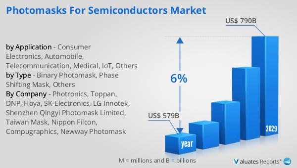
The global semiconductor market, valued at approximately $579 billion in 2022, is on a trajectory to reach around $790 billion by 2029. This growth is anticipated to occur at a compound annual growth rate (CAGR) of 6% over the forecast period. This expansion reflects the increasing demand for semiconductors across various industries, driven by technological advancements and the growing need for electronic devices. The semiconductor market is a critical component of the global economy, as semiconductors are essential for the functioning of a wide range of electronic devices, from smartphones and computers to automobiles and industrial machinery. The projected growth of the semiconductor market is supported by several factors, including the rise of the Internet of Things (IoT), the expansion of 5G networks, and the increasing adoption of artificial intelligence (AI) technologies. These trends are driving the demand for more advanced and efficient semiconductor devices, which in turn fuels the growth of the semiconductor market. Additionally, the ongoing digital transformation across various industries is contributing to the increased demand for semiconductors, as businesses and consumers alike seek to leverage technology for improved efficiency and connectivity. As the semiconductor market continues to grow, it presents significant opportunities for companies involved in the design, manufacturing, and distribution of semiconductor devices. The market's expansion also underscores the importance of innovation and development in the semiconductor industry, as companies strive to meet the evolving needs of their customers and stay competitive in a rapidly changing technological landscape.
| Report Metric | Details |
| Report Name | Photomasks for Semiconductors Market |
| Accounted market size in year | US$ 579 billion |
| Forecasted market size in 2029 | US$ 790 billion |
| CAGR | 6% |
| Base Year | year |
| Forecasted years | 2025 - 2029 |
| by Type |
|
| by Application |
|
| Production by Region |
|
| Consumption by Region |
|
| By Company | Photronics, Toppan, DNP, Hoya, SK-Electronics, LG Innotek, Shenzhen Qingyi Photomask Limited, Taiwan Mask, Nippon Filcon, Compugraphics, Newway Photomask |
| Forecast units | USD million in value |
| Report coverage | Revenue and volume forecast, company share, competitive landscape, growth factors and trends |