What is Global IC Packaging Solder Ball Market?
The Global IC Packaging Solder Ball Market is a crucial segment within the semiconductor industry, focusing on the tiny spheres of solder used to create electrical connections between integrated circuits (ICs) and printed circuit boards (PCBs). These solder balls are essential in the packaging of ICs, ensuring that the chips can be mounted onto boards with precision and reliability. The market encompasses various types of solder balls, including those made from lead and lead-free materials, catering to different technological and environmental requirements. As the demand for smaller, more efficient electronic devices grows, the need for advanced IC packaging solutions, including high-quality solder balls, becomes increasingly important. This market is driven by innovations in electronics, the push for miniaturization, and the global shift towards environmentally friendly manufacturing processes. The solder balls play a pivotal role in ensuring the performance and longevity of electronic devices, making them indispensable in the production of everything from consumer electronics to industrial machinery. As technology continues to evolve, the Global IC Packaging Solder Ball Market is expected to expand, driven by the ongoing advancements in semiconductor technology and the increasing complexity of electronic devices.
Lead Solder Ball, Lead Free Solder Ball in the Global IC Packaging Solder Ball Market:
Lead solder balls and lead-free solder balls are two primary types of solder balls used in the Global IC Packaging Solder Ball Market, each with distinct characteristics and applications. Lead solder balls, traditionally composed of a tin-lead alloy, have been widely used due to their excellent electrical conductivity, low melting point, and ease of use. These properties make them ideal for applications where reliable electrical connections are paramount, and where the manufacturing process can accommodate the use of lead. However, the use of lead in electronics has raised environmental and health concerns, leading to regulatory measures aimed at reducing or eliminating lead in electronic components. This shift has paved the way for lead-free solder balls, which are typically made from alloys such as tin-silver-copper (SAC). Lead-free solder balls offer a more environmentally friendly alternative, aligning with global initiatives to reduce hazardous substances in electronics. Despite their higher melting points and sometimes more challenging processing requirements, lead-free solder balls are increasingly favored in the industry, particularly in regions with strict environmental regulations. The transition from lead to lead-free solder balls has been driven by both regulatory pressures and the growing consumer demand for greener products. Manufacturers have invested in research and development to improve the performance of lead-free solder balls, ensuring they meet the rigorous demands of modern electronic devices. This includes enhancing their mechanical strength, thermal fatigue resistance, and overall reliability. As a result, lead-free solder balls have become a viable and often preferred option for many applications, from consumer electronics to automotive and industrial systems. The choice between lead and lead-free solder balls ultimately depends on various factors, including regulatory requirements, cost considerations, and specific application needs. In some cases, the superior performance characteristics of lead solder balls may still justify their use, particularly in high-reliability applications where the environmental impact is deemed secondary. However, the trend towards lead-free solutions is clear, driven by both legislative mandates and a broader industry commitment to sustainability. As the Global IC Packaging Solder Ball Market continues to evolve, the balance between lead and lead-free options will likely shift further towards environmentally friendly alternatives, reflecting the industry's ongoing adaptation to changing technological and regulatory landscapes. This transition is not without its challenges, as manufacturers must navigate the complexities of developing and implementing new materials and processes. However, the potential benefits in terms of environmental impact, regulatory compliance, and consumer acceptance make the pursuit of lead-free solutions a compelling and necessary endeavor for the industry.
BGA, CSP & WLCSP, Flip-Chip & Others in the Global IC Packaging Solder Ball Market:
The Global IC Packaging Solder Ball Market finds extensive usage in various packaging technologies, including Ball Grid Array (BGA), Chip Scale Package (CSP) & Wafer Level Chip Scale Package (WLCSP), Flip-Chip, and others. Each of these technologies utilizes solder balls to establish reliable electrical connections between the IC and the substrate, playing a critical role in the performance and reliability of electronic devices. BGA is a popular packaging technology that uses solder balls arranged in a grid pattern on the underside of the IC package. This configuration allows for a higher density of connections compared to traditional pin-based packages, enabling more compact and efficient designs. BGA packages are widely used in applications ranging from consumer electronics to telecommunications and automotive systems, where space and performance are critical considerations. CSP and WLCSP are advanced packaging technologies that further miniaturize the IC package, allowing for even smaller and more efficient designs. These technologies use solder balls to connect the IC directly to the substrate, eliminating the need for a separate package. This results in a thinner, lighter, and more cost-effective solution, ideal for applications where size and weight are critical factors, such as mobile devices and wearable technology. Flip-Chip technology is another important application of solder balls, where the IC is mounted upside down on the substrate, with the solder balls providing the electrical connections. This approach allows for a higher density of connections and improved thermal performance, making it suitable for high-performance applications such as processors and graphics chips. The use of solder balls in these technologies is essential for ensuring the reliability and performance of the final product, as they provide the necessary electrical and mechanical connections between the IC and the substrate. The choice of solder ball material and design can significantly impact the performance and reliability of the package, making it a critical consideration in the design and manufacturing process. As the demand for smaller, more efficient electronic devices continues to grow, the importance of advanced packaging technologies and the role of solder balls in these solutions will only increase. The Global IC Packaging Solder Ball Market is poised to benefit from these trends, as manufacturers seek to develop and implement new materials and processes that meet the evolving needs of the industry. This includes the ongoing transition to lead-free solder balls, as well as the development of new alloys and designs that offer improved performance and reliability. The market is also driven by the increasing complexity of electronic devices, which require more advanced packaging solutions to accommodate the growing number of connections and the need for improved thermal and electrical performance. As a result, the Global IC Packaging Solder Ball Market is expected to continue its growth trajectory, driven by the ongoing advancements in semiconductor technology and the increasing demand for smaller, more efficient electronic devices.
Global IC Packaging Solder Ball Market Outlook:
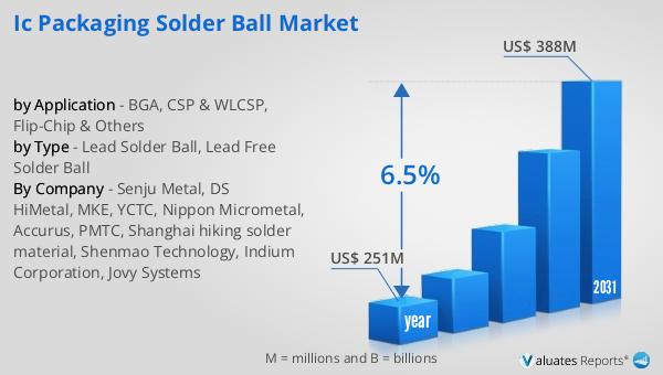
In 2024, the global market for IC Packaging Solder Balls was valued at approximately $251 million. By 2031, it is anticipated to grow to a revised size of around $388 million, reflecting a compound annual growth rate (CAGR) of 6.5% over the forecast period. This growth trajectory underscores the increasing demand for solder balls in the semiconductor industry, driven by advancements in technology and the rising need for efficient electronic packaging solutions. Key players in this market, such as Senju Metal Accurus and DS HiMetal, hold a significant portion of the market share, collectively accounting for over 73% of the global market. Their dominance highlights the competitive landscape of the industry, where innovation and quality are paramount. The market's expansion is fueled by the ongoing shift towards miniaturization and the development of environmentally friendly manufacturing processes. As electronic devices become more complex and compact, the demand for high-quality solder balls that ensure reliable electrical connections and optimal performance continues to rise. This growth is also supported by the increasing adoption of advanced packaging technologies, such as BGA, CSP, and Flip-Chip, which rely heavily on solder balls for their functionality. The market outlook reflects a dynamic and evolving industry, where the pursuit of innovation and sustainability drives the development of new materials and processes. As the global market for IC Packaging Solder Balls continues to expand, it presents significant opportunities for manufacturers and stakeholders to capitalize on the growing demand for advanced electronic packaging solutions.
| Report Metric | Details |
| Report Name | IC Packaging Solder Ball Market |
| Accounted market size in year | US$ 251 million |
| Forecasted market size in 2031 | US$ 388 million |
| CAGR | 6.5% |
| Base Year | year |
| Forecasted years | 2025 - 2031 |
| by Type |
|
| by Application |
|
| Production by Region |
|
| Consumption by Region |
|
| By Company | Senju Metal, DS HiMetal, MKE, YCTC, Nippon Micrometal, Accurus, PMTC, Shanghai hiking solder material, Shenmao Technology, Indium Corporation, Jovy Systems |
| Forecast units | USD million in value |
| Report coverage | Revenue and volume forecast, company share, competitive landscape, growth factors and trends |