What is Global Through Silicon Via (TSV) Packaging Market?
The Global Through Silicon Via (TSV) Packaging Market is a fascinating segment of the semiconductor industry that focuses on advanced packaging technologies. TSV is a method used to create vertical electrical connections (vias) through silicon wafers, enabling the stacking of multiple semiconductor dies. This technology is pivotal in enhancing the performance and efficiency of electronic devices by reducing the distance that signals must travel, thereby improving speed and reducing power consumption. TSV packaging is particularly significant in the context of miniaturization trends, as it allows for more compact and efficient designs. It is widely used in applications that require high bandwidth and low latency, such as in high-performance computing, telecommunications, and consumer electronics. The market for TSV packaging is driven by the increasing demand for smaller, faster, and more energy-efficient electronic devices. As technology continues to evolve, the role of TSV in enabling next-generation electronic products becomes increasingly critical, making it a key area of focus for semiconductor manufacturers and researchers alike.
2.5D, 3D in the Global Through Silicon Via (TSV) Packaging Market:
The concepts of 2.5D and 3D packaging are integral to understanding the Global Through Silicon Via (TSV) Packaging Market. In 2.5D packaging, multiple chips are placed side by side on an interposer, which is a piece of silicon that acts as a bridge for electrical connections. This method allows for the integration of different types of chips, such as logic and memory, on a single package, enhancing performance and reducing power consumption. The interposer provides a platform for high-density interconnections, which is crucial for applications requiring high bandwidth and low latency. On the other hand, 3D packaging involves stacking multiple semiconductor dies vertically, with TSVs providing the necessary electrical connections between the layers. This approach significantly reduces the footprint of the package, making it ideal for applications where space is at a premium. 3D packaging offers even greater performance improvements compared to 2.5D, as it allows for shorter interconnects and better thermal management. Both 2.5D and 3D packaging are essential for meeting the demands of modern electronic devices, which require ever-increasing levels of performance and efficiency. The choice between 2.5D and 3D packaging depends on various factors, including the specific requirements of the application, cost considerations, and manufacturing capabilities. As the semiconductor industry continues to push the boundaries of what is possible, the role of TSV in enabling these advanced packaging technologies becomes increasingly important. The development of 2.5D and 3D packaging technologies is driven by the need to overcome the limitations of traditional packaging methods, which are becoming increasingly inadequate in the face of growing demands for higher performance and lower power consumption. TSV technology provides a solution to these challenges by enabling the integration of multiple chips in a single package, thereby improving performance and reducing power consumption. The use of TSVs in 2.5D and 3D packaging also allows for greater design flexibility, as it enables the integration of different types of chips, such as logic, memory, and sensors, in a single package. This flexibility is crucial for meeting the diverse needs of modern electronic devices, which require a wide range of functionalities. The adoption of 2.5D and 3D packaging technologies is expected to continue to grow as the demand for high-performance, energy-efficient electronic devices increases. The development of these technologies is also supported by advances in manufacturing processes, which are making it possible to produce TSVs with smaller diameters and higher aspect ratios, thereby improving performance and reducing costs. As the semiconductor industry continues to evolve, the role of TSV in enabling advanced packaging technologies is expected to become even more significant, making it a key area of focus for researchers and manufacturers alike.
Memory Arrays, Image Sensors, Graphics Chips, MPUs (Microprocessor Units), DRAM (Dynamic Random Access Memory), Integrated Circuits, Others in the Global Through Silicon Via (TSV) Packaging Market:
The Global Through Silicon Via (TSV) Packaging Market finds extensive usage across various applications, each benefiting from the unique advantages offered by TSV technology. In memory arrays, TSVs enable the stacking of memory chips, significantly increasing storage capacity while reducing the physical footprint. This is particularly beneficial in data centers and high-performance computing environments where space and power efficiency are critical. Image sensors also leverage TSV technology to enhance performance. By stacking sensor and logic chips, TSVs help improve image processing speed and quality, which is essential for applications in smartphones, digital cameras, and surveillance systems. Graphics chips, which require high bandwidth and fast data transfer rates, benefit from TSV packaging by enabling closer integration of memory and processing units. This results in improved graphics performance, making it ideal for gaming consoles and professional graphics workstations. Microprocessor Units (MPUs) are another area where TSV technology is making a significant impact. By allowing for the integration of multiple processing cores and memory in a single package, TSVs enhance processing power and efficiency, which is crucial for modern computing applications. Dynamic Random Access Memory (DRAM) also benefits from TSV packaging, as it allows for higher memory densities and faster data access speeds. This is particularly important in applications such as servers and high-performance computing, where large amounts of data need to be processed quickly. Integrated circuits, which form the backbone of modern electronic devices, also leverage TSV technology to improve performance and reduce power consumption. By enabling the integration of multiple functions in a single package, TSVs help reduce the size and complexity of electronic devices, making them more efficient and cost-effective. Other applications of TSV technology include its use in advanced sensors, communication devices, and consumer electronics, where the demand for high performance and energy efficiency continues to grow. As the semiconductor industry continues to evolve, the role of TSV in enabling these advanced applications is expected to become even more significant, making it a key area of focus for researchers and manufacturers alike.
Global Through Silicon Via (TSV) Packaging Market Outlook:
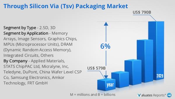
The semiconductor industry is witnessing a remarkable transformation, with the global market for semiconductors valued at approximately $579 billion in 2022. This market is projected to reach around $790 billion by 2029, reflecting a compound annual growth rate (CAGR) of 6% over the forecast period. This growth is driven by the increasing demand for advanced electronic devices that require high-performance, energy-efficient components. The rise of technologies such as artificial intelligence, the Internet of Things (IoT), and 5G is further fueling the demand for semiconductors, as these technologies rely heavily on advanced processing and connectivity capabilities. The Global Through Silicon Via (TSV) Packaging Market plays a crucial role in this growth, as it enables the development of smaller, faster, and more efficient semiconductor devices. TSV technology allows for the integration of multiple chips in a single package, improving performance and reducing power consumption. This is particularly important in applications such as high-performance computing, telecommunications, and consumer electronics, where the demand for high-speed, low-power devices is increasing. As the semiconductor industry continues to evolve, the role of TSV in enabling next-generation electronic products is expected to become even more significant, making it a key area of focus for researchers and manufacturers alike.
| Report Metric | Details |
| Report Name | Through Silicon Via (TSV) Packaging Market |
| Accounted market size in year | US$ 579 billion |
| Forecasted market size in 2029 | US$ 790 billion |
| CAGR | 6% |
| Base Year | year |
| Forecasted years | 2025 - 2029 |
| Segment by Type |
|
| Segment by Application |
|
| By Region |
|
| By Company | Applied Materials, STATS ChipPAC Ltd, Micralyne, Inc, Teledyne, DuPont, China Wafer Level CSP Co, Samsung Electronics, Amkor Technology, FRT GmbH |
| Forecast units | USD million in value |
| Report coverage | Revenue and volume forecast, company share, competitive landscape, growth factors and trends |