What is Global Semiconductor Wafers Used CMP Pad Market?
The Global Semiconductor Wafers Used CMP Pad Market is a specialized segment within the semiconductor industry that focuses on the production and utilization of Chemical Mechanical Planarization (CMP) pads. These pads are essential components in the semiconductor manufacturing process, particularly in the planarization of wafer surfaces. CMP pads are used to smooth and flatten the surface of semiconductor wafers, ensuring that subsequent layers of materials can be applied evenly. This process is crucial for the production of integrated circuits and other semiconductor devices, as it directly impacts the performance and reliability of the final products. The market for CMP pads is driven by the increasing demand for semiconductors in various applications, including consumer electronics, automotive, and telecommunications. As technology advances, the need for more sophisticated and efficient CMP pads continues to grow, making this market a vital part of the semiconductor supply chain. The market is characterized by continuous innovation and development, with manufacturers striving to produce pads that offer improved performance, longer lifespan, and reduced environmental impact. Overall, the Global Semiconductor Wafers Used CMP Pad Market plays a critical role in the advancement of semiconductor technology and the broader electronics industry.
Hard CMP Pads, Soft CMP Pads in the Global Semiconductor Wafers Used CMP Pad Market:
In the Global Semiconductor Wafers Used CMP Pad Market, there are two primary types of CMP pads: hard CMP pads and soft CMP pads. Hard CMP pads are typically made from rigid materials such as polyurethane and are designed to provide a firm and stable surface for the planarization process. These pads are known for their durability and ability to maintain a consistent level of performance over time. Hard CMP pads are often used in applications where a high degree of precision and control is required, such as in the production of advanced semiconductor devices with complex architectures. They are particularly effective in removing excess material from the wafer surface, ensuring a smooth and even finish. On the other hand, soft CMP pads are made from more flexible materials and are designed to offer a gentler touch during the planarization process. These pads are ideal for applications where a delicate approach is needed, such as in the polishing of fragile or sensitive materials. Soft CMP pads are often used in the production of semiconductor devices with less stringent requirements for surface uniformity, where the primary goal is to achieve a smooth finish without causing damage to the underlying materials. The choice between hard and soft CMP pads depends on several factors, including the specific requirements of the manufacturing process, the type of materials being used, and the desired outcome. Manufacturers must carefully consider these factors when selecting the appropriate CMP pad for their needs, as the wrong choice can lead to suboptimal results and increased production costs. In addition to hard and soft CMP pads, there are also hybrid pads that combine the characteristics of both types. These pads offer a balance between the durability and precision of hard pads and the gentleness and flexibility of soft pads. Hybrid CMP pads are often used in applications where a versatile solution is needed, allowing manufacturers to achieve the desired level of planarization without compromising on performance or quality. The development of new and improved CMP pads is an ongoing process, with manufacturers continually seeking to enhance the performance and efficiency of their products. This includes the use of advanced materials and technologies, such as nanotechnology and machine learning, to create pads that offer superior performance and longer lifespan. As the demand for semiconductors continues to grow, the need for high-quality CMP pads will remain a critical factor in the success of the Global Semiconductor Wafers Used CMP Pad Market.
300 mm Wafer, 200 mm Wafer, Others in the Global Semiconductor Wafers Used CMP Pad Market:
The usage of Global Semiconductor Wafers Used CMP Pad Market is crucial in various areas, including 300 mm wafers, 200 mm wafers, and others. The 300 mm wafer segment is one of the most significant areas of application for CMP pads, as these larger wafers are commonly used in the production of advanced semiconductor devices. The increased size of 300 mm wafers allows for more efficient manufacturing processes, as more chips can be produced from a single wafer. This efficiency is essential for meeting the growing demand for semiconductors in various industries, including consumer electronics, automotive, and telecommunications. CMP pads play a vital role in ensuring the quality and performance of 300 mm wafers, as they help to achieve the necessary level of surface planarization required for the production of high-performance semiconductor devices. The 200 mm wafer segment is another important area of application for CMP pads. Although smaller than 300 mm wafers, 200 mm wafers are still widely used in the semiconductor industry, particularly for the production of less advanced devices and applications. CMP pads are essential for maintaining the quality and consistency of 200 mm wafers, as they help to ensure that the wafer surfaces are smooth and even, allowing for the efficient application of subsequent layers of materials. The use of CMP pads in the 200 mm wafer segment is critical for achieving the desired level of performance and reliability in the final products. In addition to 300 mm and 200 mm wafers, CMP pads are also used in other areas of the semiconductor industry, including the production of specialty devices and applications. These may include smaller wafers, such as 150 mm or 100 mm wafers, as well as non-standard wafer sizes used in niche applications. The versatility and adaptability of CMP pads make them an essential component in the production of a wide range of semiconductor devices, ensuring that manufacturers can achieve the desired level of planarization and surface quality regardless of the specific requirements of their applications. The ongoing development and innovation in CMP pad technology continue to drive the growth and success of the Global Semiconductor Wafers Used CMP Pad Market, as manufacturers strive to meet the evolving needs of the semiconductor industry.
Global Semiconductor Wafers Used CMP Pad Market Outlook:
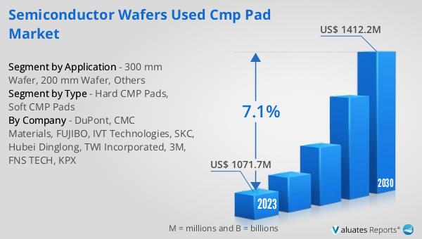
The global market for Semiconductor Wafers Used CMP Pad was valued at $996 million in 2024 and is anticipated to expand to a revised size of $1,598 million by 2031, reflecting a compound annual growth rate (CAGR) of 7.1% during the forecast period. This growth is indicative of the increasing demand for CMP pads in the semiconductor industry, driven by the rising need for advanced semiconductor devices across various sectors. The market's expansion is fueled by technological advancements and the continuous development of new and improved CMP pad materials and designs. As the semiconductor industry evolves, the demand for high-quality CMP pads that offer enhanced performance, durability, and efficiency continues to grow. This growth trajectory highlights the critical role that CMP pads play in the semiconductor manufacturing process, as they are essential for achieving the necessary level of surface planarization required for the production of high-performance semiconductor devices. The market's projected growth also underscores the importance of innovation and development in the CMP pad industry, as manufacturers strive to meet the evolving needs of their customers and maintain a competitive edge in the global market. Overall, the Global Semiconductor Wafers Used CMP Pad Market is poised for significant growth in the coming years, driven by the increasing demand for semiconductors and the continuous advancement of CMP pad technology.
| Report Metric | Details |
| Report Name | Semiconductor Wafers Used CMP Pad Market |
| Accounted market size in year | US$ 996 million |
| Forecasted market size in 2031 | US$ 1598 million |
| CAGR | 7.1% |
| Base Year | year |
| Forecasted years | 2025 - 2031 |
| by Type |
|
| by Application |
|
| Production by Region |
|
| Consumption by Region |
|
| By Company | DuPont, CMC Materials, FUJIBO, IVT Technologies, SKC, Hubei Dinglong, TWI Incorporated, 3M, FNS TECH, KPX |
| Forecast units | USD million in value |
| Report coverage | Revenue and volume forecast, company share, competitive landscape, growth factors and trends |