What is Global Wafer Handling Electrostatic Chuck Market?
The Global Wafer Handling Electrostatic Chuck Market is a specialized segment within the semiconductor industry that focuses on the development and distribution of electrostatic chucks used for wafer handling. These chucks are critical components in semiconductor manufacturing, as they securely hold silicon wafers during various processing stages, such as etching, deposition, and lithography. The market is driven by the increasing demand for semiconductors in various applications, including consumer electronics, automotive, and telecommunications. Electrostatic chucks offer several advantages over traditional mechanical clamping methods, such as reduced particle contamination, improved wafer flatness, and enhanced process uniformity. As the semiconductor industry continues to evolve with advancements in technology and the push for smaller, more efficient devices, the demand for high-performance wafer handling solutions like electrostatic chucks is expected to grow. This market encompasses a range of products, including different types of electrostatic chucks designed for specific wafer sizes and materials, catering to the diverse needs of semiconductor manufacturers worldwide. The ongoing research and development efforts in this field aim to enhance the performance and reliability of electrostatic chucks, further driving their adoption in the global market.
Coulomb Type Electrostatic Chuck, Johnsen-Rahbek (JR) Type Electrostatic Chuck in the Global Wafer Handling Electrostatic Chuck Market:
The Global Wafer Handling Electrostatic Chuck Market features two primary types of electrostatic chucks: Coulomb Type and Johnsen-Rahbek (JR) Type. Each type has distinct characteristics and applications, making them suitable for different semiconductor manufacturing processes. The Coulomb Type Electrostatic Chuck operates based on the principle of electrostatic attraction between the chuck and the wafer. It uses a dielectric material to create an electric field that holds the wafer in place. This type of chuck is known for its simplicity and reliability, making it a popular choice for various wafer handling applications. The Coulomb Type is particularly effective in environments where high clamping force is required, and it is often used in processes such as chemical vapor deposition (CVD) and physical vapor deposition (PVD). On the other hand, the Johnsen-Rahbek (JR) Type Electrostatic Chuck operates on a different principle, utilizing the Johnsen-Rahbek effect, which involves the generation of an electrostatic force through a combination of dielectric and conductive materials. This type of chuck is designed to provide a more uniform clamping force across the wafer surface, reducing the risk of wafer damage and improving process uniformity. The JR Type is particularly advantageous in applications where precise control over wafer flatness and uniformity is critical, such as in advanced lithography processes. Both types of electrostatic chucks play a crucial role in the semiconductor manufacturing process, offering unique benefits that cater to the specific needs of different applications. As the demand for more advanced semiconductor devices continues to grow, the development and adoption of these electrostatic chucks are expected to increase, driving innovation and efficiency in the global wafer handling market.
300 mm Wafer, 200 mm Wafer, Others in the Global Wafer Handling Electrostatic Chuck Market:
The Global Wafer Handling Electrostatic Chuck Market finds its application in handling various wafer sizes, including 300 mm wafers, 200 mm wafers, and others. Each wafer size presents unique challenges and requirements, making the choice of electrostatic chuck crucial for efficient semiconductor manufacturing. The 300 mm wafer is the largest standard size used in the industry, offering significant advantages in terms of cost and efficiency. Handling these larger wafers requires electrostatic chucks that can provide uniform clamping force across the entire surface, ensuring minimal wafer bowing and optimal process uniformity. The use of electrostatic chucks in 300 mm wafer processing is critical for high-volume manufacturing environments, where maximizing throughput and yield is essential. The 200 mm wafer, while smaller than the 300 mm, remains a staple in the semiconductor industry, particularly for the production of mature technology nodes and specialty devices. Electrostatic chucks used for 200 mm wafers must offer precise control over clamping force and wafer flatness to ensure high-quality processing. These chucks are often employed in applications such as MEMS (Micro-Electro-Mechanical Systems) and power devices, where maintaining tight process tolerances is crucial. In addition to the standard 300 mm and 200 mm wafers, the Global Wafer Handling Electrostatic Chuck Market also caters to other wafer sizes and materials, including smaller wafers used in niche applications and emerging technologies. The versatility of electrostatic chucks allows them to be adapted for various wafer sizes and materials, providing semiconductor manufacturers with the flexibility needed to meet diverse production requirements. As the semiconductor industry continues to evolve, the demand for advanced wafer handling solutions that can accommodate different wafer sizes and materials is expected to grow, driving innovation and development in the electrostatic chuck market.
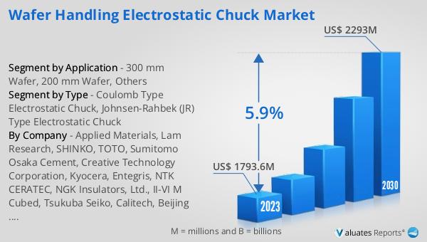
Global Wafer Handling Electrostatic Chuck Market Outlook:
The global market for Wafer Handling Electrostatic Chuck was valued at US$ 1716 million in the year 2024 and is projected to reach a revised size of US$ 2541 million by 2031, growing at a CAGR of 5.9% during the forecast period. Applied Materials dominated with a 43.84% revenue market share, followed by Lam Research with a 31.58% revenue share and SHINKO with a 10.21% revenue share. This market outlook highlights the significant growth potential of the Global Wafer Handling Electrostatic Chuck Market, driven by the increasing demand for semiconductors across various industries. The dominance of key players like Applied Materials, Lam Research, and SHINKO underscores the competitive nature of the market, with these companies leading the way in innovation and product development. As the semiconductor industry continues to expand, the need for efficient and reliable wafer handling solutions is expected to rise, further fueling the growth of the electrostatic chuck market. The projected growth rate of 5.9% CAGR indicates a steady increase in market size, reflecting the ongoing advancements in semiconductor manufacturing technology and the growing adoption of electrostatic chucks in various applications. This market outlook provides valuable insights into the future trajectory of the Global Wafer Handling Electrostatic Chuck Market, highlighting the opportunities and challenges that lie ahead for industry players.
| Report Metric | Details |
| Report Name | Wafer Handling Electrostatic Chuck Market |
| Accounted market size in year | US$ 1716 million |
| Forecasted market size in 2031 | US$ 2541 million |
| CAGR | 5.9% |
| Base Year | year |
| Forecasted years | 2025 - 2031 |
| by Type |
|
| by Application |
|
| Production by Region |
|
| Consumption by Region |
|
| By Company | Applied Materials, Lam Research, SHINKO, TOTO, Sumitomo Osaka Cement, Creative Technology Corporation, Kyocera, Entegris, NTK CERATEC, NGK Insulators, Ltd., II-VI M Cubed, Tsukuba Seiko, Calitech, Beijing U-PRECISION TECH CO., LTD. |
| Forecast units | USD million in value |
| Report coverage | Revenue and volume forecast, company share, competitive landscape, growth factors and trends |