What is Global 300 mm Wafer Shippers and Carriers Market?
The Global 300 mm Wafer Shippers and Carriers Market is a specialized segment within the semiconductor industry that focuses on the transportation and protection of 300 mm silicon wafers. These wafers are critical components in the manufacturing of semiconductors, which are used in a wide range of electronic devices. The market for these shippers and carriers is driven by the increasing demand for semiconductors, which in turn is fueled by the growing adoption of electronic devices and advancements in technology. The shippers and carriers are designed to ensure the safe handling and transportation of these delicate wafers, preventing damage and contamination. This market is characterized by the presence of a few key players who dominate the industry, providing high-quality and reliable solutions to semiconductor manufacturers. As the demand for semiconductors continues to rise, the Global 300 mm Wafer Shippers and Carriers Market is expected to grow, offering opportunities for innovation and development in the design and functionality of these essential tools.
FOUP, FOSB in the Global 300 mm Wafer Shippers and Carriers Market:
FOUP (Front Opening Unified Pod) and FOSB (Front Opening Shipping Box) are integral components of the Global 300 mm Wafer Shippers and Carriers Market. These specialized containers are designed to protect and transport 300 mm silicon wafers, which are essential in semiconductor manufacturing. FOUPs are used primarily within semiconductor fabrication facilities, or fabs, to safely store and move wafers between different processing stations. They are designed to maintain a controlled environment, protecting the wafers from contamination and physical damage. FOUPs are equipped with advanced features such as automated handling systems, which allow for seamless integration with robotic arms and other automated equipment used in modern fabs. This automation is crucial for maintaining the high throughput and precision required in semiconductor manufacturing. On the other hand, FOSBs are used for the transportation of wafers between different facilities or fabs. They are designed to provide robust protection during shipping, ensuring that the wafers arrive at their destination without any damage. FOSBs are typically made from durable materials and are equipped with features such as shock absorbers and secure locking mechanisms to prevent any movement or impact during transit. Both FOUPs and FOSBs play a critical role in the semiconductor supply chain, ensuring the safe and efficient handling of wafers from production to final assembly. The demand for these containers is driven by the increasing complexity and precision required in semiconductor manufacturing, as well as the growing global demand for electronic devices. As the semiconductor industry continues to evolve, there is a constant need for innovation in the design and functionality of FOUPs and FOSBs to meet the changing requirements of manufacturers. This includes the development of new materials and technologies that can enhance the protection and efficiency of these containers. Additionally, the trend towards automation and smart manufacturing is driving the integration of advanced features such as sensors and IoT connectivity in FOUPs and FOSBs, enabling real-time monitoring and tracking of wafers throughout the supply chain. This not only improves the efficiency of wafer handling but also enhances the overall quality and reliability of semiconductor products. As a result, the Global 300 mm Wafer Shippers and Carriers Market is poised for significant growth, offering opportunities for companies to develop innovative solutions that meet the evolving needs of the semiconductor industry.
Foundry, IDM in the Global 300 mm Wafer Shippers and Carriers Market:
The usage of Global 300 mm Wafer Shippers and Carriers Market in foundries and Integrated Device Manufacturers (IDMs) is crucial for the efficient production and handling of semiconductors. Foundries, which are specialized facilities that manufacture semiconductors for other companies, rely heavily on these shippers and carriers to ensure the safe and efficient handling of wafers throughout the production process. In foundries, FOUPs are used to transport wafers between different processing stations within the facility, maintaining a controlled environment to prevent contamination and damage. This is essential for maintaining the high quality and yield of semiconductor products. The use of automated handling systems in conjunction with FOUPs allows foundries to achieve high throughput and precision, which is critical for meeting the demands of their customers. FOSBs, on the other hand, are used for the transportation of wafers between different foundries or to other facilities for further processing or assembly. This ensures that the wafers are protected during transit and arrive at their destination in optimal condition. IDMs, which design and manufacture their own semiconductors, also rely on 300 mm wafer shippers and carriers to ensure the efficient handling of wafers throughout their production facilities. Like foundries, IDMs use FOUPs to transport wafers between different processing stations, maintaining a controlled environment to ensure the quality and reliability of their products. The use of automated handling systems in conjunction with FOUPs allows IDMs to achieve high throughput and precision, which is essential for meeting the demands of their customers. FOSBs are used by IDMs for the transportation of wafers between different facilities or to other companies for further processing or assembly. This ensures that the wafers are protected during transit and arrive at their destination in optimal condition. The demand for 300 mm wafer shippers and carriers in both foundries and IDMs is driven by the increasing complexity and precision required in semiconductor manufacturing, as well as the growing global demand for electronic devices. As the semiconductor industry continues to evolve, there is a constant need for innovation in the design and functionality of these containers to meet the changing requirements of manufacturers. This includes the development of new materials and technologies that can enhance the protection and efficiency of wafer handling. Additionally, the trend towards automation and smart manufacturing is driving the integration of advanced features such as sensors and IoT connectivity in FOUPs and FOSBs, enabling real-time monitoring and tracking of wafers throughout the supply chain. This not only improves the efficiency of wafer handling but also enhances the overall quality and reliability of semiconductor products. As a result, the Global 300 mm Wafer Shippers and Carriers Market is poised for significant growth, offering opportunities for companies to develop innovative solutions that meet the evolving needs of the semiconductor industry.
Global 300 mm Wafer Shippers and Carriers Market Outlook:
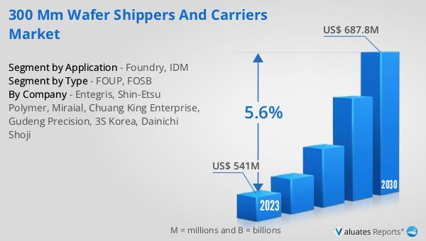
In 2024, the global market for 300 mm Wafer Shippers and Carriers was valued at approximately $521 million. This market is anticipated to expand significantly, reaching an estimated size of $759 million by 2031. This growth is expected to occur at a compound annual growth rate (CAGR) of 5.6% over the forecast period. A notable aspect of this market is the dominance of a few key players, with the top five companies collectively holding a substantial 96.32% share of the global market. This concentration indicates a highly competitive landscape where a small number of companies have established a strong foothold, likely due to their ability to provide high-quality and reliable solutions that meet the stringent requirements of the semiconductor industry. The projected growth of the market is driven by the increasing demand for semiconductors, which are essential components in a wide range of electronic devices. As technology continues to advance and the adoption of electronic devices grows, the need for efficient and reliable wafer handling solutions becomes even more critical. This presents opportunities for companies within the market to innovate and develop new products that enhance the protection and efficiency of wafer transportation and handling. The integration of advanced technologies such as automation, sensors, and IoT connectivity is expected to play a significant role in the evolution of the market, enabling real-time monitoring and tracking of wafers throughout the supply chain. This not only improves the efficiency of wafer handling but also enhances the overall quality and reliability of semiconductor products. As a result, the Global 300 mm Wafer Shippers and Carriers Market is poised for significant growth, offering opportunities for companies to develop innovative solutions that meet the evolving needs of the semiconductor industry.
| Report Metric | Details |
| Report Name | 300 mm Wafer Shippers and Carriers Market |
| Accounted market size in year | US$ 521 million |
| Forecasted market size in 2031 | US$ 759 million |
| CAGR | 5.6% |
| Base Year | year |
| Forecasted years | 2025 - 2031 |
| by Type |
|
| by Application |
|
| Production by Region |
|
| Consumption by Region |
|
| By Company | Entegris, Shin-Etsu Polymer, Miraial, Chuang King Enterprise, Gudeng Precision, 3S Korea, Dainichi Shoji |
| Forecast units | USD million in value |
| Report coverage | Revenue and volume forecast, company share, competitive landscape, growth factors and trends |