What is Global Borosilicate Glass Wafer Market?
The Global Borosilicate Glass Wafer Market is a specialized segment within the broader glass industry, focusing on the production and distribution of borosilicate glass wafers. These wafers are known for their exceptional thermal and chemical resistance, making them ideal for various high-tech applications. Borosilicate glass is composed of silica and boron trioxide, which gives it a low coefficient of thermal expansion, enhancing its durability under temperature fluctuations. This type of glass is widely used in industries such as electronics, pharmaceuticals, and scientific research due to its ability to withstand harsh environments. The market for borosilicate glass wafers is driven by the increasing demand for advanced electronic devices and the growing need for reliable materials in semiconductor manufacturing. As technology continues to evolve, the demand for borosilicate glass wafers is expected to rise, driven by their critical role in ensuring the performance and longevity of electronic components. The market is characterized by a mix of established players and emerging companies, all striving to innovate and meet the diverse needs of their customers. With ongoing advancements in technology and manufacturing processes, the Global Borosilicate Glass Wafer Market is poised for continued growth and development.
2 inch, 3 inch, 4 inch, Others in the Global Borosilicate Glass Wafer Market:
In the Global Borosilicate Glass Wafer Market, the size of the wafers plays a crucial role in determining their application and utility. The market is segmented based on wafer sizes, including 2-inch, 3-inch, 4-inch, and other sizes, each catering to specific industry needs. The 2-inch wafers are typically used in applications where space is a constraint, or where smaller components are required. These wafers are often utilized in niche markets or specialized applications, such as in certain types of sensors or microelectromechanical systems (MEMS). Their compact size allows for precision and efficiency in small-scale production environments. On the other hand, 3-inch wafers are more commonly used in the semiconductor industry, where they serve as a standard size for many manufacturing processes. These wafers provide a balance between size and functionality, making them suitable for a wide range of applications, from integrated circuits to photovoltaic cells. The 4-inch wafers, being larger, are often employed in high-volume production settings. They are favored in industries that require large-scale manufacturing capabilities, such as in the production of solar panels or large electronic displays. The larger surface area of 4-inch wafers allows for more components to be fabricated simultaneously, increasing efficiency and reducing costs. Beyond these standard sizes, the market also includes other wafer sizes that are tailored to specific customer requirements. These custom sizes are often developed in collaboration with clients to meet unique specifications or to address particular challenges in the manufacturing process. The flexibility in wafer sizing is a testament to the adaptability of the borosilicate glass wafer market, as it strives to meet the evolving demands of various industries. Each wafer size offers distinct advantages and is chosen based on the specific needs of the application, whether it be for precision, efficiency, or scalability. As technology advances and new applications emerge, the demand for different wafer sizes is expected to grow, driving innovation and competition within the market. The ability to produce wafers in a variety of sizes is a key factor in the market's success, as it allows manufacturers to cater to a diverse range of industries and applications. This versatility is essential in a rapidly changing technological landscape, where the need for specialized materials and components is constantly evolving. The Global Borosilicate Glass Wafer Market's focus on size differentiation highlights its commitment to providing tailored solutions that meet the specific needs of its customers, ensuring its continued relevance and growth in the years to come.
Semiconductor, MEMS Industry, Sensor, Others in the Global Borosilicate Glass Wafer Market:
The Global Borosilicate Glass Wafer Market finds extensive usage across several key industries, including semiconductors, MEMS, sensors, and others, each benefiting from the unique properties of borosilicate glass. In the semiconductor industry, borosilicate glass wafers are essential due to their thermal stability and resistance to chemical corrosion. These properties make them ideal substrates for the fabrication of integrated circuits and other semiconductor devices, where precision and reliability are paramount. The wafers' ability to withstand high temperatures and harsh chemical environments ensures the integrity and performance of semiconductor components, making them a critical material in this sector. In the MEMS industry, borosilicate glass wafers are used to create micro-scale devices that integrate electrical and mechanical components. The wafers' durability and precision make them suitable for the production of MEMS devices, which are used in a wide range of applications, from automotive sensors to medical devices. The ability to produce intricate and reliable components is crucial in the MEMS industry, where the demand for miniaturization and functionality continues to grow. Sensors, another key area of application, benefit from the use of borosilicate glass wafers due to their stability and resistance to environmental factors. These wafers are used in the production of various types of sensors, including pressure, temperature, and chemical sensors, where accuracy and reliability are essential. The wafers' properties ensure that sensors can operate effectively in challenging conditions, providing accurate and consistent data. Beyond these industries, borosilicate glass wafers are also used in other applications, such as in the production of optical components and scientific instruments. Their optical clarity and resistance to thermal shock make them suitable for use in lenses, mirrors, and other optical devices, where precision and performance are critical. In scientific research, borosilicate glass wafers are used in the development of experimental equipment and devices, where their durability and versatility are highly valued. The diverse range of applications for borosilicate glass wafers highlights their importance in modern technology and industry. As the demand for advanced materials continues to grow, the Global Borosilicate Glass Wafer Market is well-positioned to meet the needs of various sectors, driving innovation and development across multiple fields. The unique properties of borosilicate glass wafers make them an indispensable material in the pursuit of technological advancement and industrial progress.
Global Borosilicate Glass Wafer Market Outlook:
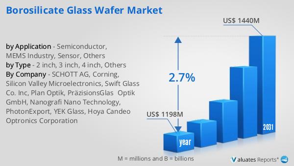
The global market for Borosilicate Glass Wafer was valued at $1,198 million in 2024 and is anticipated to expand to a revised size of $1,440 million by 2031, reflecting a compound annual growth rate (CAGR) of 2.7% over the forecast period. The Asia Pacific region, which is the largest market, experienced a decline of 2.0 percent. In contrast, sales in the Americas reached $142.1 billion, marking a significant increase of 17.0% year-on-year. Similarly, sales in Europe rose to $53.8 billion, up by 12.6% year-on-year, while Japan saw a 10.0% increase, with sales totaling $48.1 billion. However, the Asia Pacific region, despite being the largest, recorded sales of $336.2 billion, which was a 2.0% decrease year-on-year. This market outlook reflects the dynamic nature of the borosilicate glass wafer industry, with varying growth rates across different regions. The decline in the Asia Pacific region could be attributed to several factors, including market saturation or economic challenges, while the growth in the Americas, Europe, and Japan indicates a robust demand for borosilicate glass wafers in these regions. The overall market growth is driven by the increasing demand for advanced electronic devices and the need for reliable materials in semiconductor manufacturing. As the market continues to evolve, companies are focusing on innovation and expanding their product offerings to meet the diverse needs of their customers. The Global Borosilicate Glass Wafer Market is poised for continued growth, with opportunities for expansion and development across various regions and industries.
| Report Metric | Details |
| Report Name | Borosilicate Glass Wafer Market |
| Accounted market size in year | US$ 1198 million |
| Forecasted market size in 2031 | US$ 1440 million |
| CAGR | 2.7% |
| Base Year | year |
| Forecasted years | 2025 - 2031 |
| by Type |
|
| by Application |
|
| Production by Region |
|
| Consumption by Region |
|
| By Company | SCHOTT AG, Corning, Silicon Valley Microelectronics, Swift Glass Co. Inc, Plan Optik, PräzisionsGlas&Optik GmbH, Nanografi Nano Technology, PhotonExport, YEK Glass, Hoya Candeo Optronics Corporation |
| Forecast units | USD million in value |
| Report coverage | Revenue and volume forecast, company share, competitive landscape, growth factors and trends |