What is Global Photoresist for Semiconductor Market?
The Global Photoresist for Semiconductor Market is a crucial component of the semiconductor manufacturing process. Photoresists are light-sensitive materials used to form patterns on semiconductor wafers, which are essential for creating integrated circuits and other microelectronic devices. The market for these materials is driven by the increasing demand for semiconductors in various applications, including consumer electronics, automotive, and industrial sectors. As technology advances, the need for more sophisticated and miniaturized electronic components grows, further fueling the demand for high-quality photoresists. The market is characterized by continuous innovation, with manufacturers striving to develop photoresists that offer better resolution, sensitivity, and environmental compatibility. The global market for photoresists is highly competitive, with several key players dominating the industry. These companies invest heavily in research and development to maintain their competitive edge and meet the evolving needs of the semiconductor industry. Overall, the Global Photoresist for Semiconductor Market plays a vital role in the advancement of technology and the production of cutting-edge electronic devices.
Positive Photoresists, Negative Photoresists in the Global Photoresist for Semiconductor Market:
Positive and negative photoresists are two primary types of photoresists used in the semiconductor industry, each with distinct characteristics and applications. Positive photoresists become soluble when exposed to light, allowing the exposed areas to be removed during the development process. This type of photoresist is favored for its high resolution and ability to create fine patterns, making it ideal for advanced semiconductor manufacturing processes. Positive photoresists are particularly useful in applications requiring precise patterning, such as the production of microprocessors and memory devices. They offer excellent adhesion to various substrates and are compatible with different etching processes, enhancing their versatility in semiconductor fabrication. On the other hand, negative photoresists work oppositely; they become insoluble when exposed to light, meaning the unexposed areas are removed during development. Negative photoresists are known for their robustness and ability to create thicker films, making them suitable for applications where durability and thickness are critical, such as in the production of MEMS (Micro-Electro-Mechanical Systems) and certain types of sensors. While negative photoresists may not offer the same level of resolution as positive photoresists, they provide advantages in specific applications where thicker layers are required. The choice between positive and negative photoresists depends on the specific requirements of the semiconductor manufacturing process, including the desired resolution, film thickness, and compatibility with other materials and processes. Both types of photoresists are essential in the semiconductor industry, each serving unique roles in the fabrication of various electronic components. As the demand for more advanced and miniaturized electronic devices continues to grow, the development of new and improved photoresist materials remains a key focus for manufacturers. Innovations in photoresist technology aim to enhance performance, reduce environmental impact, and meet the stringent requirements of modern semiconductor manufacturing. The ongoing research and development efforts in this field are crucial for the continued advancement of the semiconductor industry and the production of next-generation electronic devices.
in the Global Photoresist for Semiconductor Market:
The Global Photoresist for Semiconductor Market finds applications in a wide range of industries, each leveraging the unique properties of photoresists to achieve specific manufacturing goals. One of the primary applications is in the production of integrated circuits (ICs), which are the building blocks of modern electronic devices. Photoresists are used to create the intricate patterns on semiconductor wafers that define the circuitry of ICs. This process is critical for the production of microprocessors, memory chips, and other essential components found in computers, smartphones, and other consumer electronics. In addition to IC manufacturing, photoresists are also used in the production of printed circuit boards (PCBs). PCBs serve as the foundation for electronic devices, providing the necessary connections between various components. Photoresists enable the precise patterning required to create the conductive pathways on PCBs, ensuring reliable performance and functionality. The automotive industry is another significant application area for photoresists, as modern vehicles increasingly rely on electronic systems for everything from engine control to infotainment systems. Photoresists play a crucial role in the production of automotive semiconductors, which are essential for the operation of these electronic systems. Furthermore, the rise of electric vehicles and autonomous driving technologies is driving demand for more advanced semiconductor components, further boosting the need for high-quality photoresists. Beyond consumer electronics and automotive applications, photoresists are also used in the production of sensors and MEMS devices. These components are critical for a wide range of applications, including industrial automation, healthcare, and environmental monitoring. Photoresists enable the precise fabrication of these devices, ensuring their accuracy and reliability in various operating conditions. As technology continues to evolve, the applications for photoresists are expanding, with new opportunities emerging in areas such as 5G telecommunications, artificial intelligence, and the Internet of Things (IoT). These technologies require advanced semiconductor components with higher performance and smaller form factors, driving the demand for innovative photoresist materials. The Global Photoresist for Semiconductor Market is poised to play a vital role in the development of these cutting-edge technologies, supporting the advancement of various industries and the creation of new opportunities for growth and innovation.
Global Photoresist for Semiconductor Market Outlook:
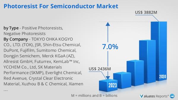
In 2024, the global Photoresist for Semiconductor Market was valued at approximately $2,585 million, with projections indicating it will grow to around $4,126 million by 2031, reflecting a compound annual growth rate (CAGR) of 7.0% over the forecast period. The market is dominated by key players such as TOK, JSR, ShinEtsu Chemical, DuPont, Fujifilm, Sumitomo Chemical, and Dongjin Semichem, which collectively accounted for about 86% of the market share in 2023. This concentration of market power underscores the competitive nature of the industry and the importance of innovation and strategic partnerships among leading manufacturers. In parallel, the broader semiconductor market was valued at $526.8 billion in 2023, with expectations to reach $780.7 billion by 2030. This growth trajectory is mirrored in the semiconductor manufacturing wafer fabrication market, which is anticipated to expand from $251.7 billion in 2023 to $506.5 billion by 2030, achieving a remarkable CAGR of 40.49% during the forecast period. These figures highlight the dynamic nature of the semiconductor industry and the critical role that photoresists play in enabling technological advancements and meeting the increasing demand for high-performance electronic components.
| Report Metric | Details |
| Report Name | Photoresist for Semiconductor Market |
| Accounted market size in year | US$ 2585 million |
| Forecasted market size in 2031 | US$ 4126 million |
| CAGR | 7.0% |
| Base Year | year |
| Forecasted years | 2025 - 2031 |
| by Type |
|
| Production by Region |
|
| Consumption by Region |
|
| By Company | TOKYO OHKA KOGYO CO., LTD. (TOK), JSR, Shin-Etsu Chemical, DuPont, Fujifilm, Sumitomo Chemical, Dongjin Semichem, Merck KGaA (AZ), Allresist GmbH, Futurrex, KemLab™ Inc, YCCHEM Co., Ltd, SK Materials Performance (SKMP), Everlight Chemical, Red Avenue, Crystal Clear Electronic Material, Xuzhou B & C Chemical, Xiamen Hengkun New Material Technology, Jiangsu Aisen Semiconductor Material, Zhuhai Cornerstone Technologies, Shanghai Sinyang Semiconductor Materials, ShenZhen RongDa Photosensitive Science & Technology, SINEVA, Guoke Tianji, Jiangsu Nata Opto-electronic Material, PhiChem, by Exposure Wavelengths, EUV Photoresists, ArF Photoresists, KrF Photoresists, g/i-Line Photoresists, Electronic Beam (EB) Photoresists |
| Forecast units | USD million in value |
| Report coverage | Revenue and volume forecast, company share, competitive landscape, growth factors and trends |


