What is Global Semiconductor Wafer-level and Advanced Packaging Inspection Systems Market?
The Global Semiconductor Wafer-level and Advanced Packaging Inspection Systems Market is a specialized segment within the semiconductor industry that focuses on the inspection and quality assurance of semiconductor wafers and advanced packaging. These systems are crucial for ensuring the reliability and performance of semiconductor devices, which are integral to a wide range of electronic products. The market encompasses various technologies and solutions designed to detect defects and ensure the integrity of semiconductor components at both the wafer level and during the packaging process. As the demand for smaller, more powerful, and energy-efficient electronic devices continues to grow, the need for advanced inspection systems becomes increasingly important. These systems help manufacturers maintain high-quality standards, reduce production costs, and improve yield rates by identifying defects early in the manufacturing process. The market is driven by technological advancements, increasing complexity of semiconductor devices, and the growing adoption of advanced packaging techniques. As a result, companies in this market are continuously innovating to develop more sophisticated inspection solutions that can meet the evolving needs of the semiconductor industry.
Optical Based, Infrared Type in the Global Semiconductor Wafer-level and Advanced Packaging Inspection Systems Market:
Optical-based and infrared-type inspection systems are two critical technologies within the Global Semiconductor Wafer-level and Advanced Packaging Inspection Systems Market. Optical-based inspection systems utilize light to detect defects on semiconductor wafers and packages. These systems employ various optical techniques, such as brightfield, darkfield, and confocal microscopy, to capture high-resolution images of the wafer surface. By analyzing these images, manufacturers can identify defects such as scratches, particles, and pattern deviations. Optical inspection is highly effective for detecting surface-level defects and is widely used in the semiconductor industry due to its non-destructive nature and ability to provide real-time feedback. On the other hand, infrared-type inspection systems leverage infrared light to penetrate deeper into the semiconductor material, allowing for the detection of subsurface defects that are not visible with optical methods. Infrared inspection is particularly useful for identifying issues such as voids, delaminations, and cracks within the wafer or package. This technology is essential for ensuring the structural integrity and reliability of semiconductor devices, especially as they become more complex and miniaturized. Both optical-based and infrared-type inspection systems play a vital role in maintaining the quality and performance of semiconductor products. As the semiconductor industry continues to evolve, the demand for advanced inspection technologies is expected to grow, driving further innovation and development in this market. Manufacturers are investing in research and development to enhance the capabilities of these systems, enabling them to detect even the smallest defects with greater accuracy and efficiency. Additionally, the integration of artificial intelligence and machine learning algorithms into inspection systems is becoming increasingly common, allowing for more sophisticated analysis and defect classification. This integration not only improves the accuracy of defect detection but also enhances the overall efficiency of the inspection process. As a result, semiconductor manufacturers can achieve higher yield rates, reduce production costs, and deliver high-quality products to the market. The Global Semiconductor Wafer-level and Advanced Packaging Inspection Systems Market is poised for significant growth as the demand for advanced electronic devices continues to rise. With the increasing complexity of semiconductor devices and the adoption of advanced packaging techniques, the need for reliable and efficient inspection systems is more critical than ever. Companies operating in this market are focused on developing innovative solutions that can meet the evolving needs of the semiconductor industry, ensuring the continued success and growth of this vital sector.
OSAT, IDM, Foundry in the Global Semiconductor Wafer-level and Advanced Packaging Inspection Systems Market:
The Global Semiconductor Wafer-level and Advanced Packaging Inspection Systems Market plays a crucial role in various areas of the semiconductor industry, including OSAT (Outsourced Semiconductor Assembly and Test), IDM (Integrated Device Manufacturer), and Foundry. In the OSAT sector, inspection systems are essential for ensuring the quality and reliability of semiconductor devices during the assembly and testing phases. OSAT companies provide assembly and testing services to semiconductor manufacturers, and the use of advanced inspection systems helps them maintain high-quality standards and meet the stringent requirements of their clients. By detecting defects early in the process, OSAT companies can reduce the risk of product failures and improve yield rates, ultimately enhancing their competitiveness in the market. In the IDM sector, inspection systems are integrated into the manufacturing process to ensure the quality and performance of semiconductor devices from design to production. IDMs are responsible for the entire semiconductor manufacturing process, from design and fabrication to assembly and testing. The use of advanced inspection systems allows IDMs to identify defects at various stages of production, enabling them to implement corrective actions and optimize their manufacturing processes. This not only improves product quality but also reduces production costs and time-to-market. In the Foundry sector, inspection systems are used to ensure the quality of semiconductor wafers produced for various clients. Foundries are specialized manufacturing facilities that produce semiconductor wafers for other companies, and the use of advanced inspection systems is critical for maintaining high-quality standards and meeting the diverse needs of their clients. By detecting defects early in the wafer production process, foundries can improve yield rates and reduce the risk of product failures, ultimately enhancing their reputation and competitiveness in the market. Overall, the Global Semiconductor Wafer-level and Advanced Packaging Inspection Systems Market is essential for ensuring the quality and reliability of semiconductor devices across various sectors of the industry. As the demand for advanced electronic devices continues to grow, the need for reliable and efficient inspection systems is more critical than ever. Companies operating in this market are focused on developing innovative solutions that can meet the evolving needs of the semiconductor industry, ensuring the continued success and growth of this vital sector.
Global Semiconductor Wafer-level and Advanced Packaging Inspection Systems Market Outlook:
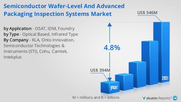
In 2024, the global market for Semiconductor Wafer-level and Advanced Packaging Inspection Systems was valued at approximately $394 million. By 2031, it is anticipated to expand to a revised size of around $546 million, reflecting a compound annual growth rate (CAGR) of 4.8% over the forecast period. This growth trajectory underscores the increasing demand for advanced inspection systems in the semiconductor industry, driven by the need for high-quality, reliable semiconductor devices. The market's expansion is fueled by technological advancements and the growing complexity of semiconductor devices, which necessitate more sophisticated inspection solutions. Notably, North America, Europe, and Japan collectively hold a significant market share of 23%, highlighting the importance of these regions in the global semiconductor landscape. The presence of leading semiconductor manufacturers and technological innovators in these regions contributes to their substantial market share. As the semiconductor industry continues to evolve, the demand for advanced inspection systems is expected to rise, driving further growth in this market. Companies operating in this space are focused on developing innovative solutions that can meet the evolving needs of the semiconductor industry, ensuring the continued success and growth of this vital sector.
| Report Metric | Details |
| Report Name | Semiconductor Wafer-level and Advanced Packaging Inspection Systems Market |
| Accounted market size in year | US$ 394 million |
| Forecasted market size in 2031 | US$ 546 million |
| CAGR | 4.8% |
| Base Year | year |
| Forecasted years | 2025 - 2031 |
| by Type |
|
| by Application |
|
| Production by Region |
|
| Consumption by Region |
|
| By Company | KLA, Onto Innovation, Semiconductor Technologies & Instruments (STI), Cohu, Camtek, Intekplus |
| Forecast units | USD million in value |
| Report coverage | Revenue and volume forecast, company share, competitive landscape, growth factors and trends |