What is Global GaAs Epitaxial Wafers Market?
The Global GaAs Epitaxial Wafers Market refers to the worldwide industry focused on the production and distribution of gallium arsenide (GaAs) epitaxial wafers. These wafers are a crucial component in the semiconductor industry, known for their superior electron mobility and ability to operate at higher frequencies compared to silicon-based wafers. GaAs epitaxial wafers are primarily used in the manufacturing of devices that require high-speed and high-frequency performance, such as radio frequency (RF) amplifiers, optoelectronic devices, and integrated circuits. The market is driven by the increasing demand for advanced communication technologies, including 5G networks and satellite communications, which require components that can handle high data rates and frequencies. Additionally, the growing adoption of GaAs wafers in the production of LEDs and solar cells further propels market growth. The market is characterized by continuous technological advancements and innovations aimed at improving wafer quality and reducing production costs. Key players in the market are investing in research and development to enhance the performance and efficiency of GaAs wafers, thereby expanding their application scope across various industries.
in the Global GaAs Epitaxial Wafers Market:
In the Global GaAs Epitaxial Wafers Market, various types of wafers are utilized by different customers based on their specific needs and applications. The primary types include semi-insulating GaAs wafers and semi-conducting GaAs wafers. Semi-insulating GaAs wafers are predominantly used in RF applications due to their high resistivity, which minimizes signal loss and interference. These wafers are essential in the production of RF amplifiers, switches, and other components used in wireless communication devices, radar systems, and satellite communications. On the other hand, semi-conducting GaAs wafers are primarily used in optoelectronic applications. They are integral in the manufacturing of devices such as laser diodes, photodetectors, and light-emitting diodes (LEDs). These wafers offer excellent electron mobility and direct bandgap properties, making them ideal for high-efficiency light emission and detection. Additionally, GaAs wafers are also used in the production of solar cells, particularly in space applications where high efficiency and radiation resistance are critical. The choice of wafer type depends on the specific requirements of the application, such as frequency range, power handling capability, and environmental conditions. Customers in the telecommunications industry, for instance, prioritize wafers that can support high-frequency operations and withstand harsh environmental conditions. In contrast, customers in the optoelectronics industry focus on wafers that offer high efficiency in light emission and detection. The market also sees a growing demand for customized GaAs wafers, where manufacturers tailor the wafer specifications to meet the unique needs of their clients. This customization includes adjustments in wafer thickness, doping levels, and surface finish to optimize performance for specific applications. The increasing complexity of electronic devices and the push for miniaturization further drive the demand for high-quality GaAs wafers. As devices become smaller and more integrated, the need for wafers that can deliver high performance in compact form factors becomes more pronounced. This trend is particularly evident in the consumer electronics sector, where the demand for smaller, faster, and more efficient devices continues to rise. Moreover, the automotive industry is emerging as a significant consumer of GaAs wafers, driven by the growing adoption of advanced driver-assistance systems (ADAS) and autonomous driving technologies. These applications require high-frequency components capable of processing large amounts of data in real-time, making GaAs wafers an ideal choice. The market is also witnessing increased collaboration between wafer manufacturers and device manufacturers to develop next-generation GaAs wafers that can meet the evolving demands of various industries. This collaboration is crucial in ensuring that the wafers produced are not only high-performing but also cost-effective and scalable for mass production. Overall, the Global GaAs Epitaxial Wafers Market is characterized by a diverse range of wafer types, each catering to the specific needs of different customers and applications. The continuous advancements in technology and the growing demand for high-performance electronic devices are expected to drive further innovation and growth in this market.
RF Field, Optoelectronic Devices, Others in the Global GaAs Epitaxial Wafers Market:
The usage of Global GaAs Epitaxial Wafers Market spans several critical areas, including the RF field, optoelectronic devices, and other applications. In the RF field, GaAs epitaxial wafers are highly valued for their ability to operate at high frequencies and provide superior performance compared to traditional silicon wafers. They are extensively used in the production of RF amplifiers, switches, and mixers, which are essential components in wireless communication systems, radar systems, and satellite communications. The high electron mobility and low noise characteristics of GaAs wafers make them ideal for these applications, where signal integrity and efficiency are paramount. In optoelectronic devices, GaAs epitaxial wafers play a crucial role in the manufacturing of laser diodes, photodetectors, and LEDs. The direct bandgap properties of GaAs allow for efficient light emission and detection, making these wafers a preferred choice for high-performance optoelectronic applications. Laser diodes made from GaAs wafers are used in a wide range of applications, including fiber optic communications, barcode scanners, and medical devices. Photodetectors and LEDs based on GaAs wafers are also widely used in consumer electronics, automotive lighting, and display technologies. Beyond RF and optoelectronic applications, GaAs epitaxial wafers are also used in the production of solar cells, particularly for space applications. The high efficiency and radiation resistance of GaAs solar cells make them ideal for use in satellites and other space-based systems, where reliability and performance are critical. Additionally, GaAs wafers are used in the development of high-speed integrated circuits and microwave monolithic integrated circuits (MMICs), which are essential for advanced communication systems and radar applications. The versatility and superior performance characteristics of GaAs epitaxial wafers make them a valuable component in a wide range of applications, driving their demand across various industries. As technology continues to advance and the demand for high-performance electronic devices grows, the usage of GaAs epitaxial wafers is expected to expand further, offering new opportunities for innovation and growth in the market.
Global GaAs Epitaxial Wafers Market Outlook:
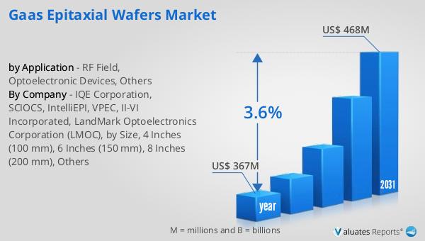
The global market for GaAs Epitaxial Wafers was valued at $367 million in 2024 and is anticipated to grow to a revised size of $468 million by 2031, reflecting a compound annual growth rate (CAGR) of 3.6% during the forecast period. The Asia Pacific region, which is the largest market for GaAs epitaxial wafers, experienced a decline of 2.0 percent. In contrast, sales in the Americas reached $142.1 billion, marking a significant year-on-year increase of 17.0%. Similarly, sales in Europe rose to $53.8 billion, up 12.6% year-on-year, while sales in Japan increased to $48.1 billion, reflecting a 10.0% year-on-year growth. Despite the overall growth in these regions, the Asia Pacific market saw a decrease in sales, totaling $336.2 billion, down 2.0% year-on-year. This market outlook highlights the dynamic nature of the GaAs epitaxial wafers market, with varying growth rates across different regions. The increasing demand for high-performance electronic devices and the continuous advancements in technology are expected to drive further growth in the market, offering new opportunities for innovation and expansion.
| Report Metric | Details |
| Report Name | GaAs Epitaxial Wafers Market |
| Accounted market size in year | US$ 367 million |
| Forecasted market size in 2031 | US$ 468 million |
| CAGR | 3.6% |
| Base Year | year |
| Forecasted years | 2025 - 2031 |
| by Application |
|
| Production by Region |
|
| Consumption by Region |
|
| By Company | IQE Corporation, SCIOCS, IntelliEPI, VPEC, II-VI Incorporated, LandMark Optoelectronics Corporation (LMOC), by Size, 4 Inches (100 mm), 6 Inches (150 mm), 8 Inches (200 mm), Others |
| Forecast units | USD million in value |
| Report coverage | Revenue and volume forecast, company share, competitive landscape, growth factors and trends |