What is Global Thick Film Photoresist Market?
The Global Thick Film Photoresist Market is a specialized segment within the broader photoresist industry, focusing on materials used in the fabrication of electronic components. These photoresists are essential in the manufacturing processes of semiconductors and other electronic devices, where they serve as a light-sensitive material that helps in the etching and patterning of circuits on substrates. The market is driven by the increasing demand for advanced electronic devices, which require precise and reliable manufacturing techniques. Thick film photoresists are particularly valued for their ability to create high-resolution patterns and their compatibility with various substrates, making them indispensable in the production of complex electronic components. As technology continues to advance, the need for more sophisticated and efficient photoresist materials grows, propelling the market forward. The global market for thick film photoresists is characterized by a high level of competition, with key players investing heavily in research and development to innovate and improve product offerings. This market is also influenced by regional production capabilities, with certain areas like Japan leading in production due to their advanced technological infrastructure and expertise in electronics manufacturing.
Thick Film Positive Photoresists, Thick Film Negative Photoresists in the Global Thick Film Photoresist Market:
Thick Film Positive Photoresists and Thick Film Negative Photoresists are two primary types of photoresist materials used in the Global Thick Film Photoresist Market, each serving distinct roles in the photolithography process. Positive photoresists become soluble when exposed to light, allowing the exposed areas to be washed away during development. This characteristic makes them ideal for applications requiring high precision and fine patterning, as they can accurately replicate intricate designs on substrates. Positive photoresists are commonly used in the production of microelectronic devices, where precision is paramount. On the other hand, Thick Film Negative Photoresists work oppositely; they become insoluble when exposed to light, meaning the unexposed areas are removed during development. This property makes negative photoresists suitable for applications where durability and robustness are required, as they tend to form thicker and more resilient layers. Negative photoresists are often used in applications such as printed circuit boards (PCBs) and other electronic components that require strong adhesion and resistance to environmental factors. Both types of photoresists are crucial in the electronics industry, each offering unique advantages that cater to different manufacturing needs. The choice between positive and negative photoresists depends on the specific requirements of the application, such as the desired resolution, thickness, and environmental resistance. As the demand for more advanced electronic devices continues to grow, the need for high-quality thick film photoresists will also increase, driving further innovation and development in this market segment. Manufacturers are continually exploring new formulations and technologies to enhance the performance of both positive and negative photoresists, ensuring they meet the evolving needs of the electronics industry. This ongoing innovation is essential for maintaining competitiveness in the global market, as companies strive to offer products that deliver superior performance and reliability. The interplay between positive and negative photoresists highlights the complexity and diversity of the Global Thick Film Photoresist Market, underscoring the importance of these materials in modern electronics manufacturing.
Wafer-Level Packaging, Flip Chip (FC), Others in the Global Thick Film Photoresist Market:
The Global Thick Film Photoresist Market finds extensive usage in various areas, including Wafer-Level Packaging, Flip Chip (FC), and other applications. Wafer-Level Packaging (WLP) is a process where the packaging of semiconductor devices is done at the wafer level, rather than after the individual chips are cut from the wafer. This method offers several advantages, such as reduced size and weight, improved performance, and lower production costs. Thick film photoresists play a crucial role in WLP by enabling the precise patterning and etching required to create the intricate structures needed for effective packaging. The ability of thick film photoresists to produce high-resolution patterns and their compatibility with various substrates make them ideal for this application. In Flip Chip (FC) technology, thick film photoresists are used to create the bumps or pillars that connect the chip to the substrate. This method of interconnection offers several benefits, including improved electrical performance, better thermal management, and increased reliability. The use of thick film photoresists in FC technology ensures that the bumps are accurately formed and adhere well to the substrate, which is critical for the overall performance of the device. Other applications of thick film photoresists include the production of microelectromechanical systems (MEMS), sensors, and other advanced electronic components. In these applications, the ability of thick film photoresists to create precise and durable patterns is essential for the functionality and reliability of the final product. The versatility and performance of thick film photoresists make them indispensable in the manufacturing of a wide range of electronic devices, from consumer electronics to industrial and automotive applications. As the demand for more advanced and miniaturized electronic components continues to grow, the importance of thick film photoresists in these applications will only increase. Manufacturers are continually developing new formulations and technologies to enhance the performance of thick film photoresists, ensuring they meet the evolving needs of the electronics industry. This ongoing innovation is crucial for maintaining competitiveness in the global market, as companies strive to offer products that deliver superior performance and reliability. The diverse applications of thick film photoresists highlight their critical role in modern electronics manufacturing, underscoring the importance of these materials in enabling the development of next-generation electronic devices.
Global Thick Film Photoresist Market Outlook:
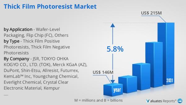
In 2024, the global market for Thick Film Photoresist was valued at approximately $146 million, with projections indicating a growth to around $215 million by 2031. This growth represents a compound annual growth rate (CAGR) of 5.8% over the forecast period. The market is dominated by the top three manufacturers, who collectively hold over 80% of the market share, highlighting the competitive nature of this industry. Japan stands out as the largest producer of thick layer photoresists, accounting for more than 55% of the global production. This dominance is attributed to Japan's advanced technological infrastructure and expertise in electronics manufacturing, which have positioned it as a leader in the production of high-quality photoresist materials. Following Japan, Europe and North America also play significant roles in the market, contributing to the global supply of thick film photoresists. The market's growth is driven by the increasing demand for advanced electronic devices, which require precise and reliable manufacturing techniques. As technology continues to evolve, the need for more sophisticated and efficient photoresist materials grows, propelling the market forward. The competitive landscape of the Global Thick Film Photoresist Market is characterized by ongoing innovation and development, as manufacturers strive to offer products that deliver superior performance and reliability. This dynamic market environment underscores the importance of thick film photoresists in modern electronics manufacturing, highlighting their critical role in enabling the development of next-generation electronic devices.
| Report Metric | Details |
| Report Name | Thick Film Photoresist Market |
| Accounted market size in year | US$ 146 million |
| Forecasted market size in 2031 | US$ 215 million |
| CAGR | 5.8% |
| Base Year | year |
| Forecasted years | 2025 - 2031 |
| by Type |
|
| by Application |
|
| Production by Region |
|
| Consumption by Region |
|
| By Company | JSR, TOKYO OHKA KOGYO CO., LTD. (TOK), Merck KGaA (AZ), DuPont, Shin-Etsu, Allresist, Futurrex, KemLab™ Inc, Youngchang Chemical, Everlight Chemical, Crystal Clear Electronic Material, Kempur Microelectronics Inc, Xuzhou B & C Chemical |
| Forecast units | USD million in value |
| Report coverage | Revenue and volume forecast, company share, competitive landscape, growth factors and trends |